
Method of embedding a pre-assembled unit including a device into a flexible printed circuit and corresponding assembly

Active Publication Date: 2014-09-18
SUMITOMO ELECTRIC PRINTED CIRCUITS INC +1
View PDF5 Cites 39 Cited by
  • Summary
  • Abstract
  • Description
  • Claims
  • Application Information

AI Technical Summary

Benefits of technology

The present invention provides a method and assembly for embedding an electronic device into a flexible printed circuit board. The method involves removing parts of the circuit to create an opening, and using an insulating material to isolate the conductive layers. The electronic device is then attached to the circuit using a thermally conductive adhesive, with the conductive connections connecting to the first conductive layer. The opening is filled with a filler material. The assembly includes two flexible printed circuits, with one circuit containing a device that is connected to the other circuit's conductive traces. The two circuits are connected at a specific point to allow for optimal thermal and electrical performance. Overall, the invention provides a flexible solution for embedding electronic devices into printed circuit boards.

Problems solved by technology

However, as more layers of metal and non-conductive substrates are added to the sandwich, the flexible printed circuit becomes less flexible.
In addition, attempts to add electrical or electronic devices require the mounting of components onto the surfaces of the flexible circuit.
Issues such as the complexity of inclusion process, high mechanical stresses, poor yield, poor thermal management, and high cost prevented inclusions of components inside FR4 for products.
Bendable regions of a flex circuit generally do not contain surface mounted component because of bending stresses could be exerted on solder joints that could lead to disruptions of electrical paths.
Today's multi-component system is not optimized for size and weight parameters.
Furthermore, the combined PCB—flex manufacturing process is complex and expensive.
Designs for flat heat sinks and bendable heat sinks are complex and limited.
The process for inclusion of SMDs is likewise complex and less cost effective.
For example, over-molding of devices such as semiconductor circuits, requires additional packaging and assembly processes.
In addition, the aforementioned PCB substrates are poor conductors of heat.
Therefore, when heat generated by the mounted device is excessive, e.g., in the case of power circuits, microprocessors, and light-emitting devices, more expensive thermally conductive substrates accompanied with the attachment of a bulky conducting heat sink are required.
The heat sink is typically metallic copper or aluminum and its attachment to the substrate or package makes the assembly bulky, heavy, and inflexible.

Method used


Image

  • Method of embedding a pre-assembled unit including a device into a flexible printed circuit and corresponding assembly
  • Method of embedding a pre-assembled unit including a device into a flexible printed circuit and corresponding assembly
  • Method of embedding a pre-assembled unit including a device into a flexible printed circuit and corresponding assembly

Examples


Embodiment Construction

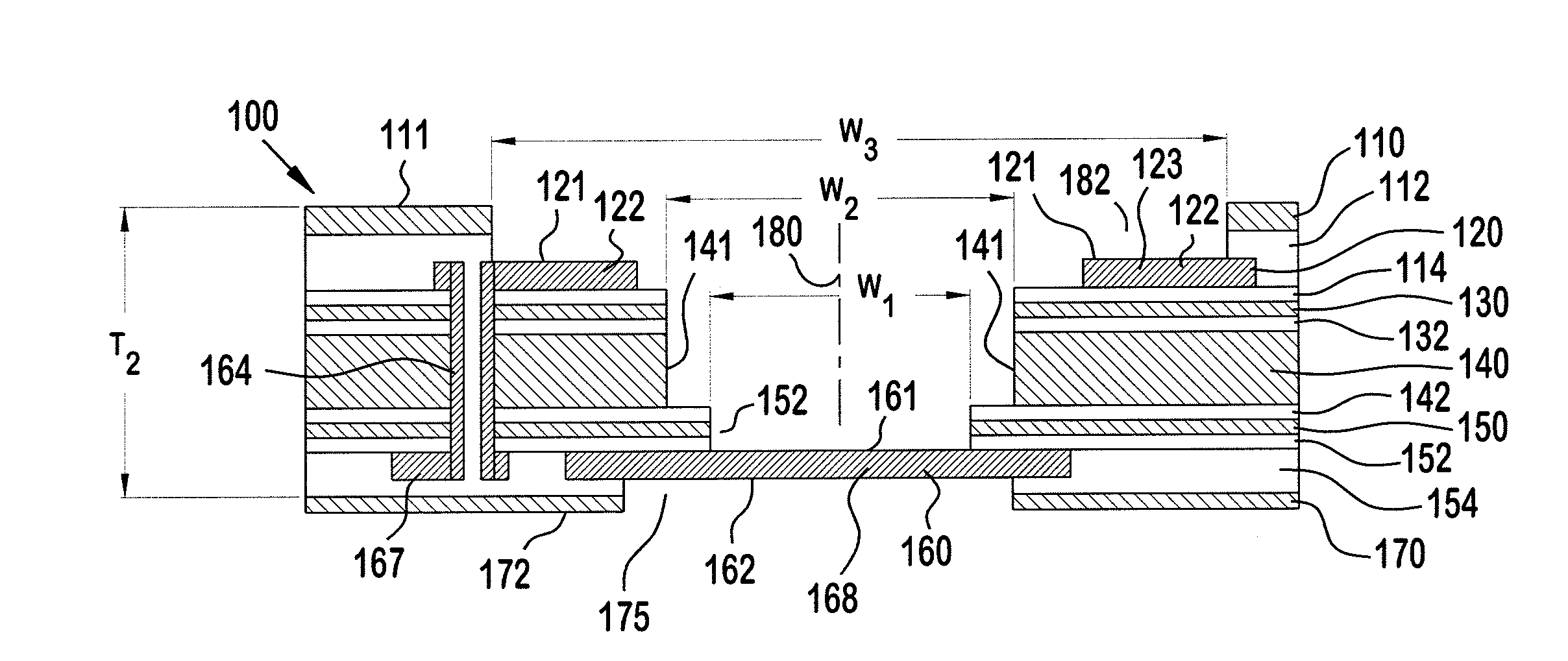
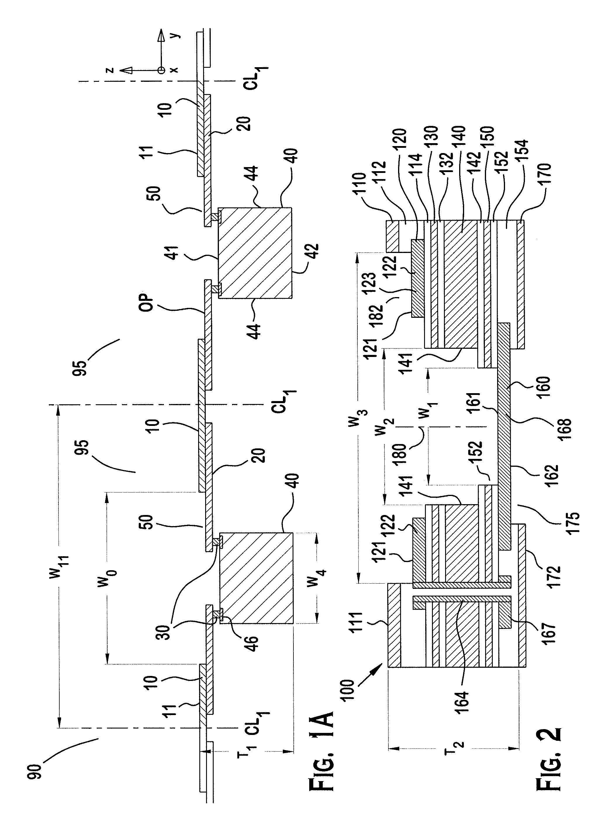
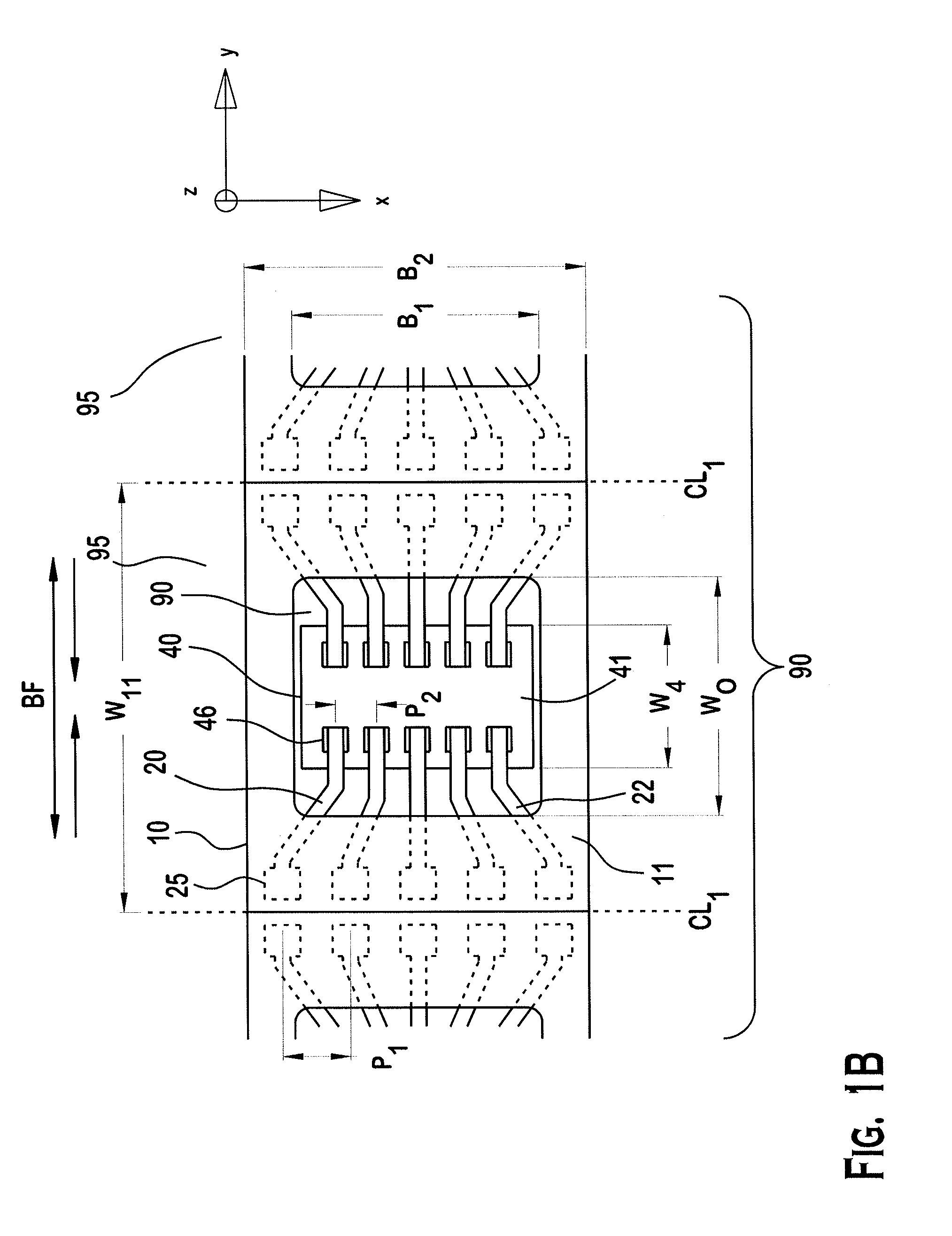
[0006]According to a first aspect of the present invention, a method of embedding an electronic device into a flexible pre-assembled printed circuit board is provided. Preferably, the method includes the steps of providing a flexible printed circuit having a first conductive layer, an insulating center layer, and a second conductive layer, the insulating center layer arranged in-between the first and the second conductive layers, the first conductive layer and the insulating center layer being removed at a predefined location to form an opening to expose an upper surface of the second conductive layer, and providing a pre-assembled electronic device including an electronic circuit and conductive connections that are connected to the electronic circuit. Moreover, the method further preferably includes the steps of providing a thermally conducting adhesive on the upper surface of the second conductive layer, providing a conductive material on an upper surface of the first conductive l...


PUM

PropertyMeasurementUnit
Lengthaaaaaaaaaa
Flexibilityaaaaaaaaaa
Electrical conductoraaaaaaaaaa

Abstract

A flexible printed circuit assembly, having a first flexible printed circuit having a first conductive layer and a device that is connected the first conductive layer; and a second flexible printed circuit having a second conductive layer, an insulating center layer, and a third conductive layer, the insulating center layer arranged in-between the second and the third conductive layers, the second conductive layer and the insulating center layer being removed to form an opening to expose an upper surface of the third conductive layer, wherein the first flexible printed circuit is arranged such that the device is accommodated inside the opening, a lower surface of the device being in thermal connection with the third conductive layer, and the first conductive layer is arranged to be in electrical connection with the second conductive layer.

Description

TECHNICAL FIELD OF THE INVENTION[0001]The present invention relates generally to flexible printed circuit assemblies including electronic devices and components embedded therein such that flexibility of the printed circuit of the assembly is maintained, and a method of embedding an electronic device or other component into the flexible printed circuit.BACKGROUND OF THE INVENTION[0002]Flexible printed circuits and rigid-flexible printed circuits are used in many applications where at least certain parts of the circuits need to be installed in a curved or bent state. Flexible printed circuits incorporate metal lines sandwiched between non-conductive flexible layers of flexible printed circuit. However, as more layers of metal and non-conductive substrates are added to the sandwich, the flexible printed circuit becomes less flexible. In addition, attempts to add electrical or electronic devices require the mounting of components onto the surfaces of the flexible circuit. The surface mo...

Claims


Application Information

Patent Timeline
IPC IPC(8): H05K1/02H05K13/04
CPCH05K1/0283H05K1/189H01L2224/83192H05K1/0207H05K1/183H05K2201/09781H05K2201/10681Y10T29/49146
Inventor WANG, JAMES JEN-HOPARK, JIN JOOKOUCHI, MASAHIKO
Owner SUMITOMO ELECTRIC PRINTED CIRCUITS INC
Learn More