Stable lithium niobate waveguide devices, and methods of making and using same

Active Publication Date: 2014-09-18
THE AEROSPACE CORPORATION
View PDF2 Cites 28 Cited by
  • Summary
  • Abstract
  • Description
  • Claims
  • Application Information

AI Technical Summary

Benefits of technology

The present invention provides lithium niobate waveguide devices that have improved stability. The devices have a unique design that prevents the formation and redistribution of surface charges that may interfere with the applied electric field in the waveguide. This is achieved by embedding an optical waveguide in a Z-cut lithium niobate substrate, and disposing signal and guard electrodes on the upper surface of the substrate. A conductive layer on the lower surface of the substrate serves as a common ground electrode for the signal and guard electrodes, keeping the electric fields induced by the electrodes away from the surface of the device. The devices can be used in optical communication systems and are stable over time.

Problems solved by technology

One choice encountered in designing a lithium niobate-based modulator is the orientation of the crystal axes relative to the waveguides and electrodes, which affects the modulator efficiency.
X-cut based modulators are particularly susceptible to charge accumulation on the surface of the crystal.
As a consequence, the outgoing light from the modulator also may deviate from the optimal output over time.
However, the monitoring circuitry required to adjust the applied voltage may add significant expense and complexity to the modulator circuit, may limit the switching speed of the device, and may limit the environments in which the device may be used.
Furthermore, as the applied DC bias steadily increases, the electric field between the device electrodes may damage the device materials during long-term operation, particularly at higher temperature.
Such damage may further accelerate the DC drift and lead to further degradation in the optical performance of the modulator.
McBrien further discloses that in Z-cut embodiments, the bias electrodes must be positioned above the optical waveguides to achieve the required electric field configuration, but that such an arrangement results in excessive optical loss.
McBrien discloses that splitting the bias electrodes into two sections may reduce the optical loss, but results in a trade-off with modulation efficiency.

Method used


Image

  • Stable lithium niobate waveguide devices, and methods of making and using same
  • Stable lithium niobate waveguide devices, and methods of making and using same
  • Stable lithium niobate waveguide devices, and methods of making and using same

Examples


Embodiment Construction
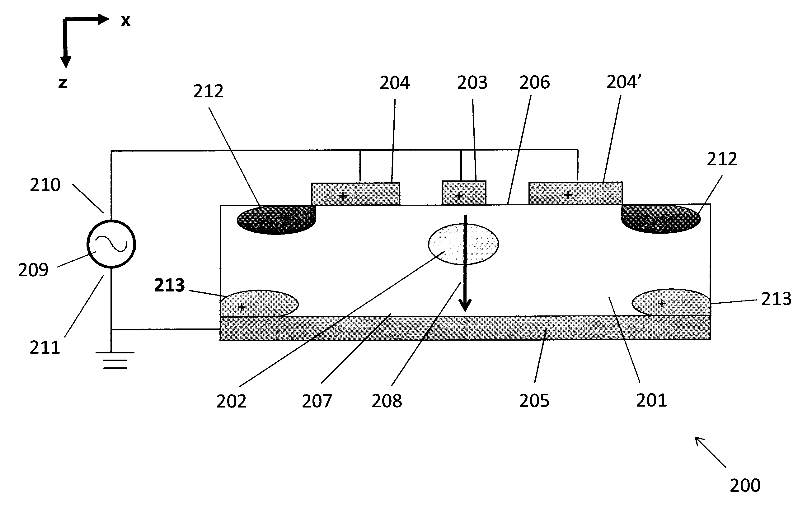
[0038]Overview

[0039]Embodiments of the present invention provide lithium niobate waveguide devices having a signal electrode and guard electrodes disposed on the upper surface of a Z-cut lithium niobate substrate, and a ground electrode disposed on the lower surface of the lithium niobate substrate. Preferably, the ground electrode is disposed beneath the signal and guard electrodes, and indeed may substantially cover the entire lower surface of the substrate. A first bias may be applied between the signal electrode and the ground electrode, so as to modulate the refractive index of a waveguide disposed therebetween. Concurrently, a second bias (which may be the same as the first bias) may be applied between each of the guard electrodes and the ground electrode. Such an arrangement may inhibit generation of space charges at the Z-surface of the crystal near the waveguide. Moreover, the guard electrodes may draw any mobile charges away from the signal electrodes, thus inhibiting drif...


PUM

PropertyMeasurementUnit
Thicknessaaaaaaaaaa
Thicknessaaaaaaaaaa
Nanoscale particle sizeaaaaaaaaaa

Abstract

Embodiments of the present invention provide stable lithium niobate waveguide devices, and methods of making and using the same. A lithium niobate-based waveguide device may include a Z-cut lithium niobate substrate having upper and lower surfaces, an optical waveguide embedded within the lithium niobate substrate, a signal electrode disposed on the upper surface of lithium niobate substrate and parallel to the optical waveguide, guard electrodes disposed on the upper surface of the lithium niobate substrate and flanking but spaced apart from the signal electrode, and a conductive layer on the lower surface of the lithium niobate substrate, wherein the conductive layer serves as a common ground reference for the signal and guard electrodes.

Description

FIELD OF THE INVENTION[0001]This application generally relates to lithium niobate waveguide devices, and methods of making and using the same.BACKGROUND OF THE INVENTION[0002]Electro-optically active waveguide devices, such as modulators, have been prepared using lithium niobate (LiNbO3). Lithium niobate has a lattice structure in which the lithium ions have a non-centrosymmetric position. In the absence of an electric field, this non-centrosymmetric position imparts the material with a net polarization. Applying an electric field to the lithium niobate shifts the position of the lithium ions, changing the net polarization, and refractive index, of the material. Thus, the phase of light propagating through the material may be altered by applying an electric field to the material.[0003]FIGS. 1A-1B schematically illustrate plan and cross-sectional views, respectively, of a previously known lithium niobate waveguide device 100 that includes lithium niobate substrate 101 in which wavegu...

Claims


Application Information

Patent Timeline
IPC IPC(8): G02F1/01
CPCG02F1/0115G02F1/0316G02F1/035G02F2202/20Y10T29/49016G02F1/212
Inventor MULLER, HEINRICH G.STAPLETON, ANDREW D.
Owner THE AEROSPACE CORPORATION
Why Eureka
Try Eureka