Resonating element, resonator, electronic device, electronic apparatus, moving vehicle and method of manufacturing resonating element

a technology of resonators and components, applied in the field of resonators, can solve the problems of reducing the effective area reducing the rigidity of the vibrating portion, and deteriorating the impact resistance or the like, so as to achieve the effect of simple processing step, impact resistance, and resistance to vibration

Inactive Publication Date: 2014-10-09
SEIKO EPSON CORP
View PDF0 Cites 1 Cited by
  • Summary
  • Abstract
  • Description
  • Claims
  • Application Information

AI Technical Summary

Benefits of technology

[0033]According to this configuration, it is possible to suppress spreading of stress occurring when bonding or fixing the vibrating element and to obtain a vibrating element having excellent frequency-temperature characteristics and CI-temperature characteristics.Application Example 13
[0037]According to this configuration, by selecting an electronic device based on the demands of a customer, it is possible to make the most of the vibrating element of the application example described above. For example, it is possible to obtain a compact and high frequency (for example, in the 490 MHz band) electronic device having excellent frequency reproducibility, frequency-temperature characteristics, and frequency-aging characteristics.
[0050]According to this manufacturing method, it is possible to manufacture the vibrating element of the application example described above by a simple processing step. For example, by forming desired thick-walled portions at optional positions on the front and rear principal surfaces, a vibrating element in which the vibrating portion is supported tightly and which is resistant to vibration, impact, or the like can be manufactured easily.

Problems solved by technology

However, there is a problem in that when the vibrating portion is made thinner, the rigidity of the vibrating portion decreases, and the impact resistance or the like deteriorates.
However, it is confirmed that there is a problem in that when this etching residue is generated, the effective area of the vibrating portion decreases, and a CI value of a main vibration mode and the ratio (CIs / CIm) of a CI value (CIs) of an adjacent spurious vibration mode to the CI value (CIm) of a main vibration mode or the like does not satisfy a standard value (for example, 1.8 or more).

Method used


Image

  • Resonating element, resonator, electronic device, electronic apparatus, moving vehicle and method of manufacturing resonating element
  • Resonating element, resonator, electronic device, electronic apparatus, moving vehicle and method of manufacturing resonating element
  • Resonating element, resonator, electronic device, electronic apparatus, moving vehicle and method of manufacturing resonating element

Examples


third embodiment

of Vibrating Element

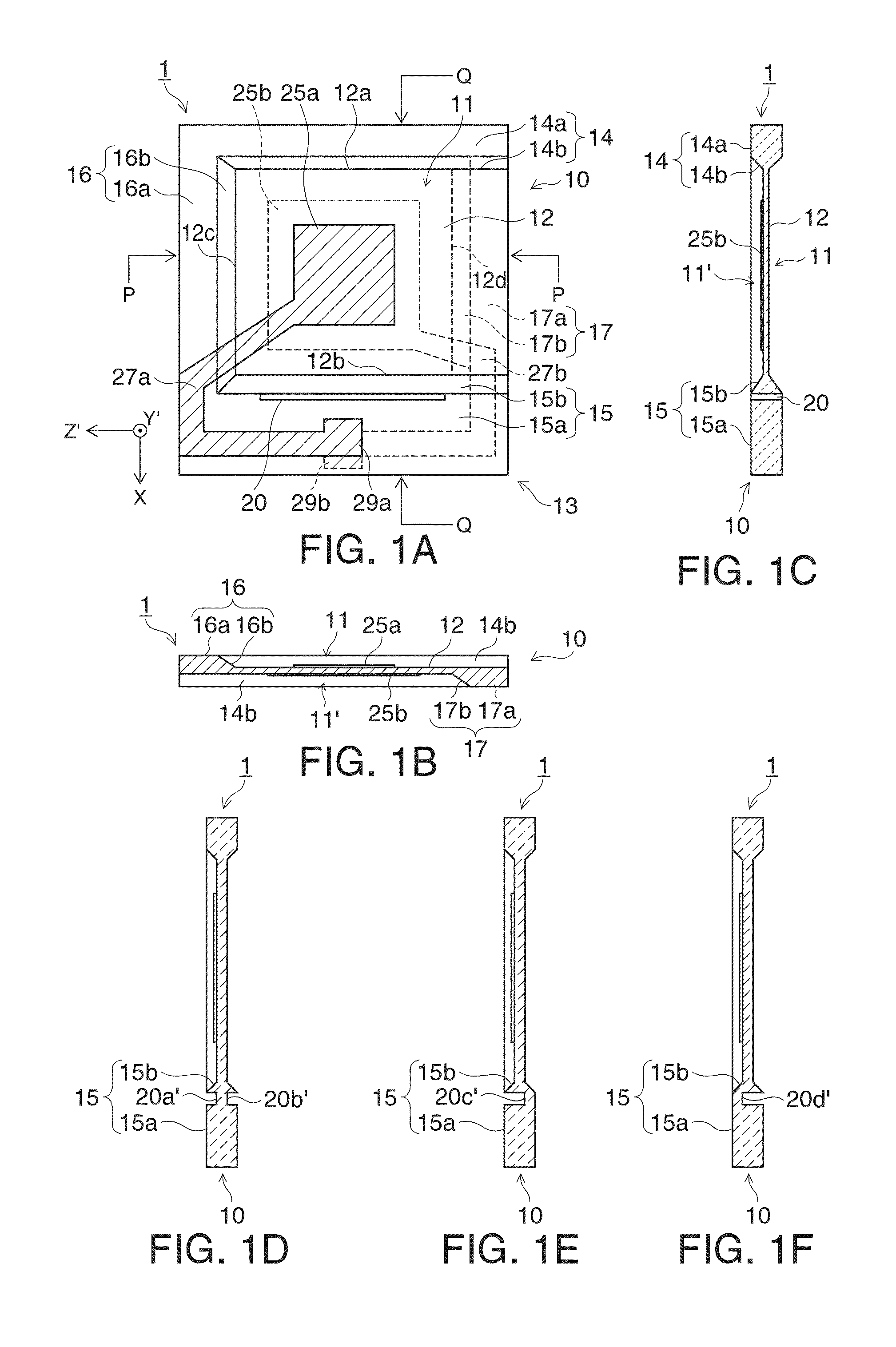
[0134]FIGS. 6A to 6C are schematic views illustrating the structure of a piezoelectric vibrating element 3 according to a third embodiment. FIG. 6A is a plan view of the piezoelectric vibrating element 3, FIG. 6B is a cross-sectional view of a P-P cross-section as seen from the positive X-axis direction, and FIG. 6C is a cross-sectional view of a Q-Q cross-section as seen from the positive Z′-axis direction.

[0135]The piezoelectric vibrating element 3 is different from the piezoelectric vibrating element 1 illustrated in FIGS. 1A to 1F in that two stress-mitigating slits 20a and 20b are formed in parallel in the third thick-walled portion 15. That is, the first slit 20a is formed in the plane of the third thick-walled body 15a, and the second slit 20b is formed in the plane of the third slope portion 15b.

[0136]By forming individual slits in the plane of the third thick-walled body 15a and the plane of the third slope portion 15b, respectively, it is possible to b...

fourth embodiment

of Vibrating Element

[0138]FIGS. 8A to 8F are schematic views illustrating the structure of a piezoelectric vibrating element 4 according to a fourth embodiment. FIG. 8A is a plan view of the piezoelectric vibrating element 4, FIG. 8B is a cross-sectional view of a P-P cross-section as seen from a positive X-axis direction, and FIG. 8C is a cross-sectional view of a Q-Q cross-section as seen from a positive Z′-axis direction.

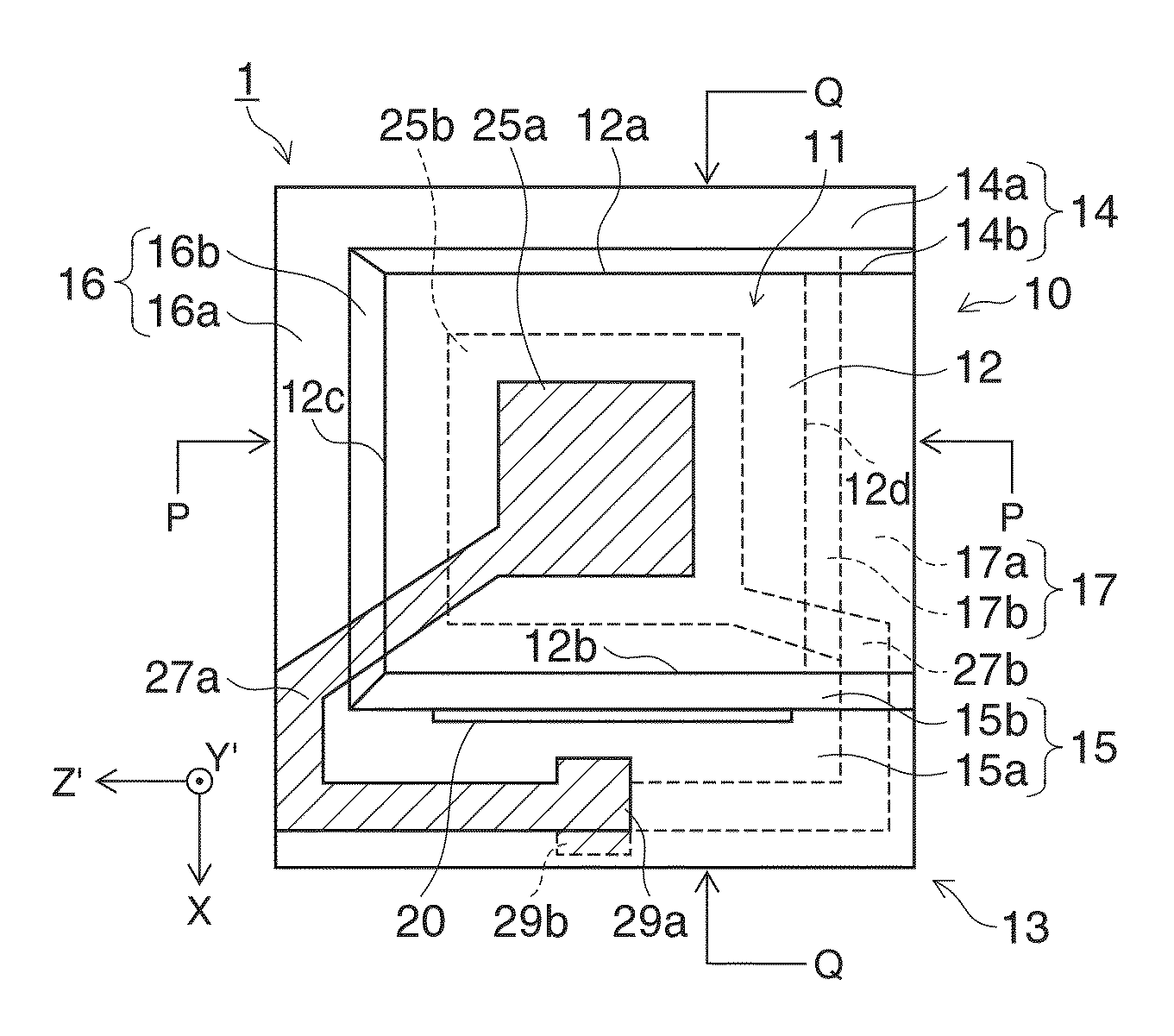
[0139]The piezoelectric vibrating element 4 includes a piezoelectric substrate 10 including a vibrating portion 12 having a thin-walled rectangular vibrating region and a thick-walled portion 13 having a thickness greater than that of the vibrating portion 12, integrated with the vibrating portion 12, excitation electrodes 25a and 25b formed on the front and rear surfaces (both principal surfaces) of the vibrating portion 12, respectively, and lead electrodes 27a and 27b that respectively extend from the excitation electrodes 25a and 25b toward pad electrodes 29a...

fifth embodiment

of Vibrating Element

[0171]FIGS. 12A to 12C are schematic views illustrating the structure of a piezoelectric vibrating element 6 according to a fifth embodiment. FIG. 12A is a plan view of the piezoelectric vibrating element 6, FIG. 12B is a cross-sectional view of a P-P cross-section as seen from the positive X-axis direction, and FIG. 12C is a cross-sectional view of a Q-Q cross-section as seen from the positive Z′-axis direction.

[0172]The piezoelectric vibrating element 6 is different from the piezoelectric vibrating element 4 illustrated in FIGS. 8A to 8F in that the stress-mitigating slit 20 is formed at a different position. In this embodiment, the slit 20 penetrates through the third slope portion 15b that is separated from the edge of the side 12a of the thin-walled vibrating portion 12. Unlike the piezoelectric vibrating element 4, the slit 20 is formed so as to be separated from both edges of the third slope portion 15b rather than forming the slit 20 in the third slope po...


PUM

PropertyMeasurementUnit
frequency-aging characteristicsaaaaaaaaaa
angleaaaaaaaaaa
temperatureaaaaaaaaaa

Abstract

A piezoelectric resonating element includes a piezoelectric substrate having a rectangular vibrating portion and a thick-walled portion, excitation electrodes and, and lead electrodes. The thick-walled portion includes a fourth thick-walled portion, a third thick-walled portion, a first thick-walled portion, and a second thick-walled portion. The third thick-walled portion includes a third slope portion and a third thick-walled body, and at least one slit is formed in the third thick-walled portion.

Description

CROSS-REFERENCE TO RELATED APPLICATIONS[0001]This is continuation application of U.S. application Ser. No. 13 / 587,252 filed Aug. 16, 2012 which claims priority to Japanese Patent Application Nos. 2012-131639 filed Jun. 11, 2012, 2011-182245 filed Aug. 24, 2011 and 2011-178783 filed Aug. 18, 2011, all of which are incorporated by reference herein in their entireties.BACKGROUND[0002]1. Technical Field[0003]The invention relates to a resonator that excites a thickness-shear vibration mode, and more particularly, to a resonating element having a so-called inverted mesa structure, a resonator, an electronic device, and an electronic apparatus using the resonator, a moving vehicle using the resonator, and a method of manufacturing the vibrating element.[0004]2. Related Art[0005]An AT-cut quartz crystal resonator which is an example of a resonator is used in various fields such as in a piezoelectric oscillator and an electronic apparatus since it excites a thickness-shear vibration mode as...

Claims


Application Information

Patent Timeline
Patent Type & Authority Applications(United States)
IPC IPC(8): H01L41/047H01L41/08
CPCH03H9/0542H03H9/0552H03H9/1021H01L41/08H03H9/132H03H9/19H01L41/047H03H9/131Y10T29/42H10N30/87H10N30/00
Inventor ISHII, OSAMUMURAKAMI, SHIRO
Owner SEIKO EPSON CORP
Why Eureka
Try Eureka