Method of Manufacturing Semiconductor Device

a manufacturing method and semiconductor technology, applied in semiconductor/solid-state device manufacturing, basic electric elements, electric devices, etc., can solve the problems of increasing the difficulty of completely removing the underlying pad oxide, reducing the breakdown voltage of the device being fabricated, and affecting the quality of the device. , to achieve the effect of improving the gate oxid

Active Publication Date: 2014-10-09
SHANGHAI HUALI MICROELECTRONICS CORP
View PDF1 Cites 2 Cited by
  • Summary
  • Abstract
  • Description
  • Claims
  • Application Information

AI Technical Summary

Benefits of technology

[0006]It is therefore an object of the present invention to address the silicon nitride residues issue of the prior art so as to morphologically improve a gate oxide and hence the reliability of the high-voltage semiconductor device being fabricated by presenting a method of manufacturing a semiconductor device.

Problems solved by technology

Such residues will cause defects in subsequent process steps and increase the difficulty to completely remove an underlying pad oxide.
This will lead to a border of the active area with sharp corners after a gate oxide is grown, thus decreasing the breakdown voltage of the device being fabricated and deteriorating its gate oxide integrity (GOI) performance.

Method used


Image

  • Method of Manufacturing Semiconductor Device
  • Method of Manufacturing Semiconductor Device
  • Method of Manufacturing Semiconductor Device

Examples


Embodiment Construction

[0032]The present invention provides a method of manufacturing a semiconductor device. To further describe the method of the invention, reference is made to the following detailed description of exemplary embodiments, taken in conjunction with the accompanying drawings. Features and advantages of the invention will be apparent from the following detailed description, and from the claims. Note that all the drawings are presented in a very simple form and not drawn precisely to scale. They are provided solely to facilitate the description of the exemplary embodiments of the invention in a convenient and clear way.

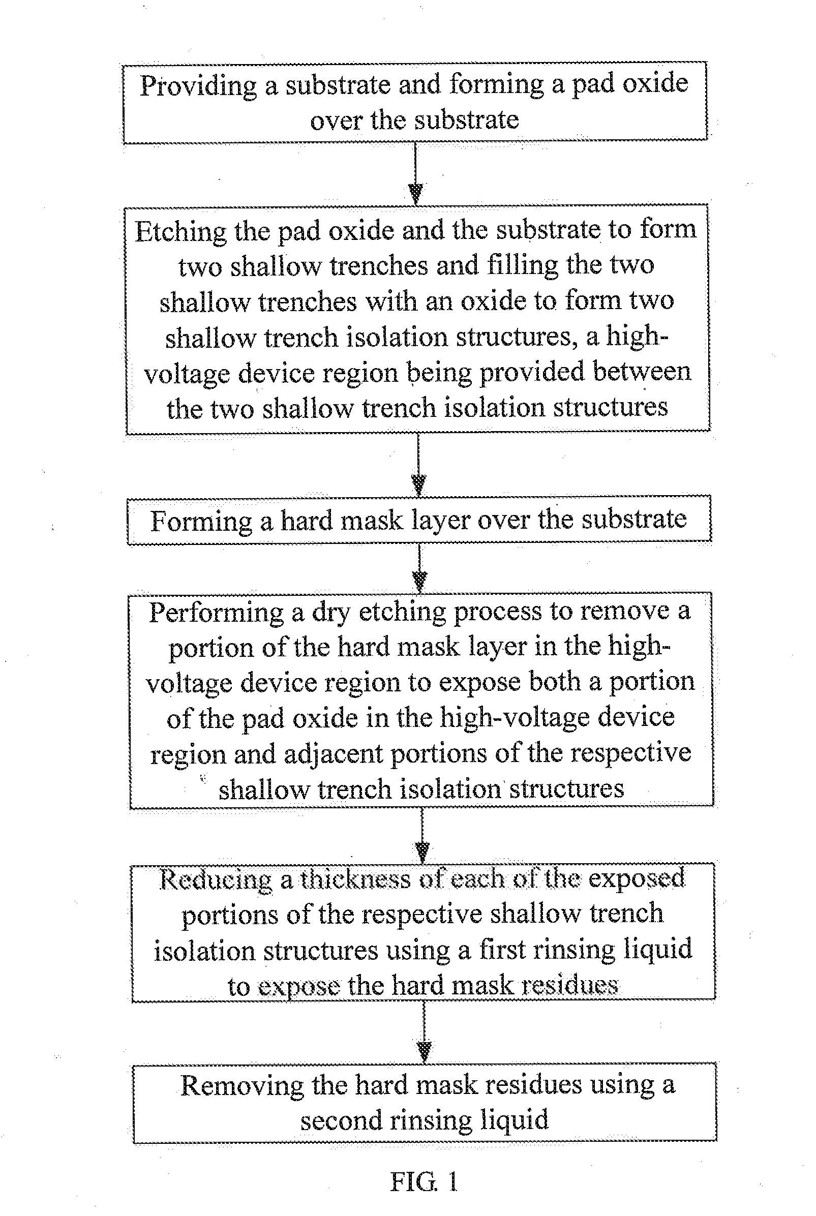
[0033]FIG. 1 is a flowchart graphically illustrating a method of manufacturing a semiconductor device in accordance with an embodiment of the present invention.

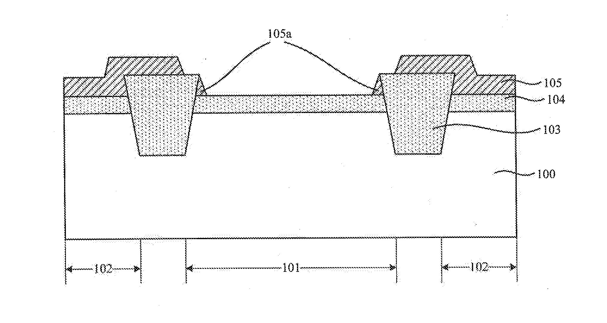
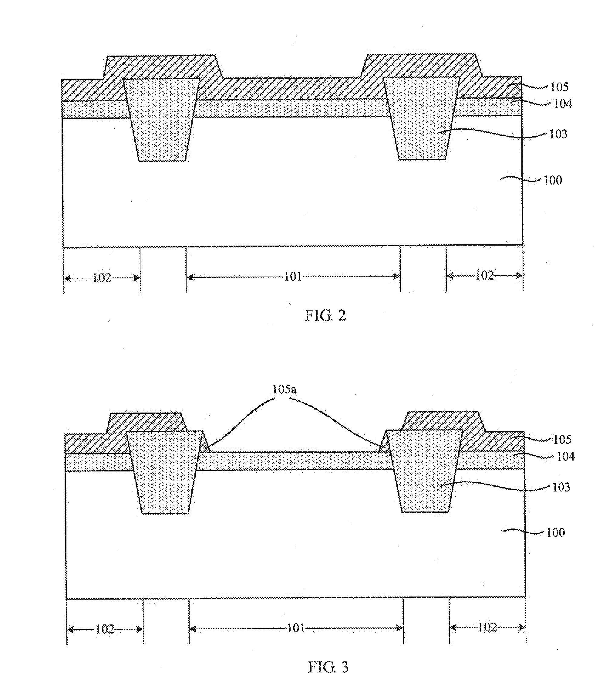
[0034]Reference is given to FIGS. 2 to 7 below to describe in further detail process steps of a method of manufacturing a semiconductor device in accordance with an embodiment of the present invention.

[0035]Referring f...


PUM


Abstract

A method of manufacturing a semiconductor device is disclosed, which can completely remove hard mask residues left along boundaries between a high-voltage device region and STI structures after a dry etch process, by partially reducing a thickness of each of the exposed portion of the respective STI structures adjacent to the high-voltage device region so as to sufficiently expose the residues. As a result, after a portion of an Underlying pad oxide corresponding to the high-voltage device region is removed in a subsequent process, the exposed surface of the substrate is uniform with a smooth and clear border. Therefore, no sharp corners will emerge at a border of a gate oxide subsequently grown on the exposed surface of the substrate, and the gate oxide is thus morphologically improved, thereby resulting in an improvement of the reliability of the high-voltage semiconductor device being fabricated.

Description

CROSS-REFERENCES TO RELATED APPLICATIONS[0001]This application claims the priority of Chinese patent application number 201310122105.X, filed on Apr. 9, 2013, the entire contents of which are incorporated herein by reference.TECHNICAL FIELD[0002]The present invention relates generally to the field of integrated circuit (IC) fabrication, and more particularly, to a method of manufacturing a semiconductor device.BACKGROUND[0003]High-voltage integrated circuits have been widely used in panel display, communications circuitry, automobile electronics and many other applications. Such a high-voltage integrated circuit typically includes a low-voltage logic section and a high-voltage section which operates under the control of a signal output from the low-voltage logic section and thereafter shifted to a high voltage level after passing through a high-voltage driver circuit containing high-voltage devices.[0004]In general, a high-voltage integrated circuit includes both high-voltage device...

Claims


Application Information

Patent Timeline
Patent Type & Authority Applications(United States)
IPC IPC(8): H01L21/762
CPCH01L21/76224H01L21/32
Inventor MA, XUZHOU, WEICAO, YAMIN
Owner SHANGHAI HUALI MICROELECTRONICS CORP
Why Eureka
Try Eureka