

Chopper amplifier
- Summary
- Abstract
- Description
- Claims
- Application Information
AI Technical Summary
Benefits of technology
Problems solved by technology
Method used
Image

Examples
first embodiment
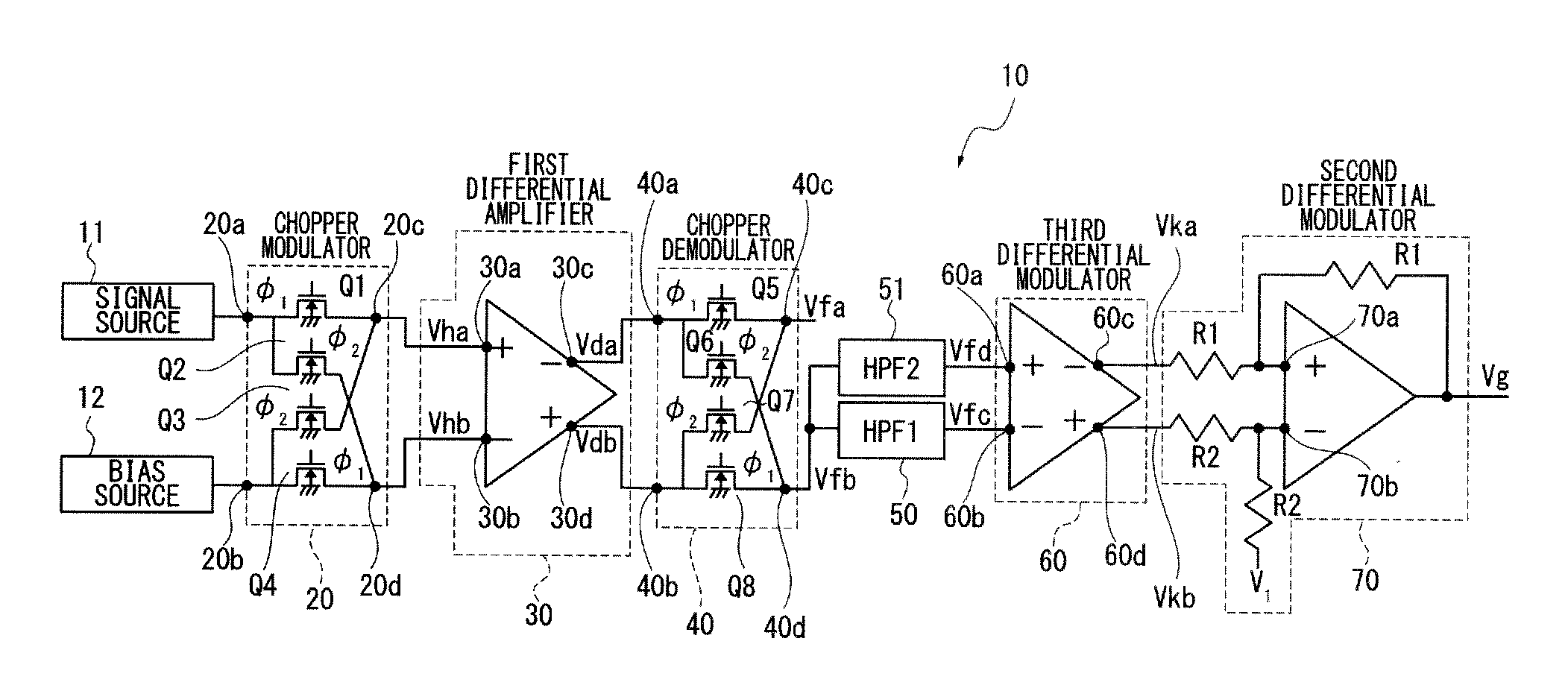
[0026]FIG. 1 shows the structure of a chopper amplifier 10. The chopper amplifier 10 comprises a chopper modulator 20 to modulate a detection signal from a signal source 11 and a bias voltage as a certain DC voltage from a bias source 12 and a differential amplifier 30 to differentially amplify a voltage or chopper modulation signal output from the chopper modulator 20.
[0027]The chopper amplifier 10 further comprises a chopper demodulator 40 to demodulate a differential output voltage from the first differential amplifier 30 and output a demodulation signal, first and second highpass filters 50, 51 to cut off a low frequency component of the demodulation signal from the chopper demodulator 40 and output a modulation signal, a third differential amplifier 60 to differentially amplify the modulation signal from the highpass filters 50, 51, and a second differential amplifier 70 to differentially amplify a differential modulation signal from the third differential amplifier 60.
[0028]Th...
second embodiment
[0055]Another example of first and second highpass filters are described referring to FIG. 4. First and second highpass filters comprise capacitors C1, C2 and MOS transistors Tr1, Tr2, respectively.
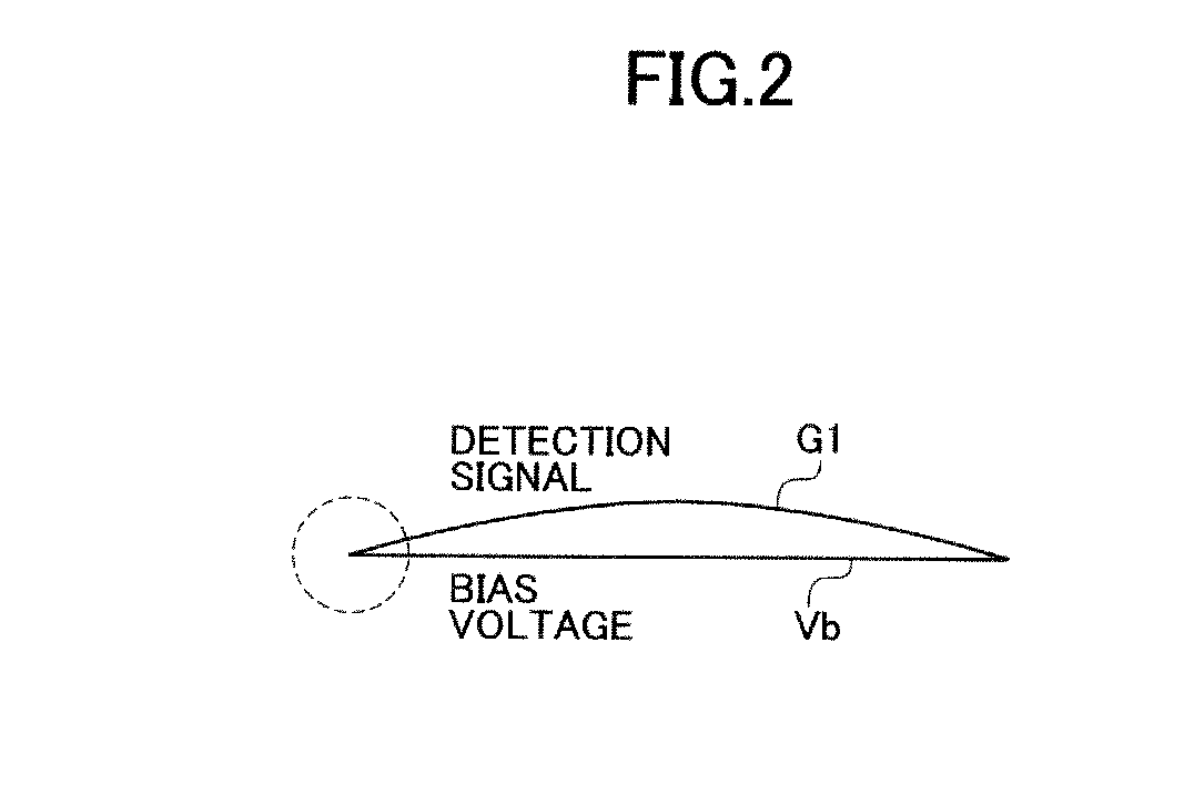
[0056]The cutoff frequency of the first highpass filter needs to be set to a low value due to the low frequency band of the detection signal G1. For example, considering the capacitance and resistance of a 1st order highpass filter with cutoff frequency of 1 Hz, when capacitance is set to 1 pF, the highpass filter requires resistance of 160 GΩ. In general a resistance of 160 GΩ made of a polysilicon element on a semiconductor substrate requires an enormous area.
[0057]In view of this, to realize a highpass filter with a smaller area and a low cutoff frequency, a very large-resistance element can be formed by setting a gate-source voltage Vgs of the MOS transistor Tr1 to a threshold voltage or less. This is because the smaller the voltage Vgs, the larger the resistance the MOS transistor Tr...
PUM
 Abstract
Description
Claims
Application Information