Silicon target for sputtering film formation and method for forming silicon-containing thin film

a technology of sputtering film and silicon, which is applied in the direction of electrolysis components, vacuum evaporation coatings, coatings, etc., can solve the problems of deteriorating film quality and abnormal electrical discharge during sputtering, and achieve the effect of reducing the charge-up during sputtering film formation

Active Publication Date: 2014-10-30
SHIN ETSU CHEM IND CO LTD
View PDF4 Cites 0 Cited by
  • Summary
  • Abstract
  • Description
  • Claims
  • Application Information

AI Technical Summary

Benefits of technology

[0018]In the present invention, the conductive layer made of the material having a smaller work function than that of the n-type silicon target material is provided on the bonding surface of the target material. Accordingly, charge-up during sputtering film formation is reduced, and dust generation is inhibited. As a result, a high-quality silicon-containing thin film can be formed.

Problems solved by technology

When the target material has high electric resistance, abnormal electrical discharge such as arc discharge may occur during sputtering.
The generated dust causes a defect in the formed silicon-containing thin film, and thereby deteriorates the film quality.

Method used


Image

  • Silicon target for sputtering film formation and method for forming silicon-containing thin film
  • Silicon target for sputtering film formation and method for forming silicon-containing thin film
  • Silicon target for sputtering film formation and method for forming silicon-containing thin film

Examples


example

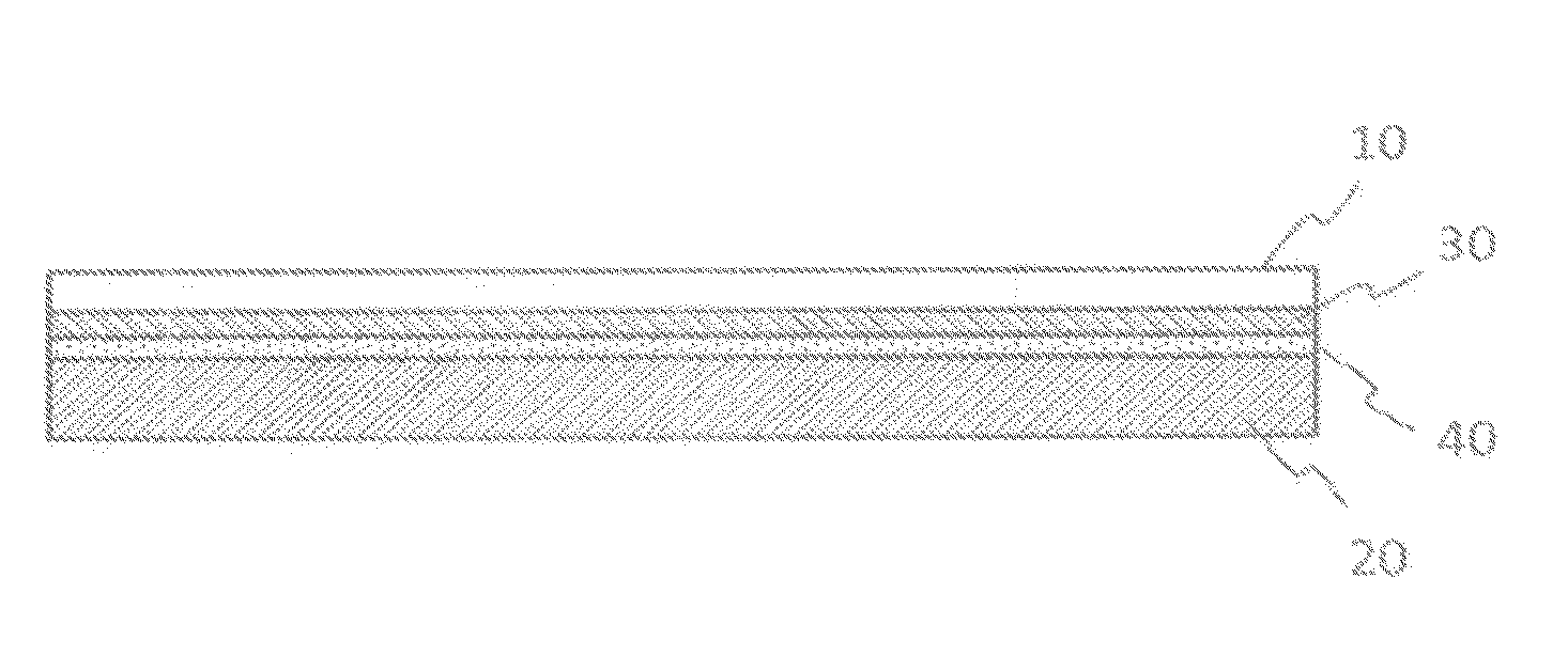
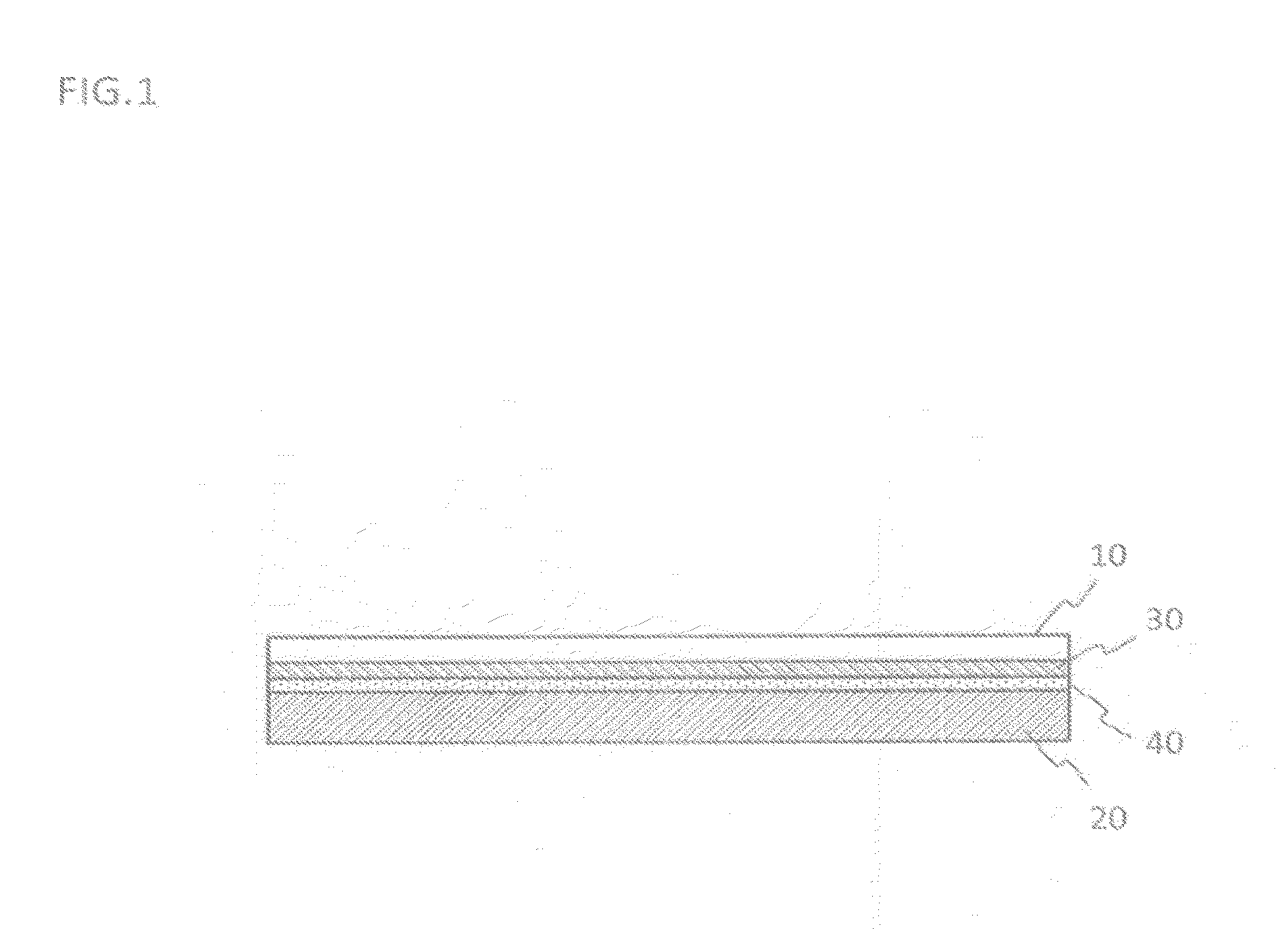
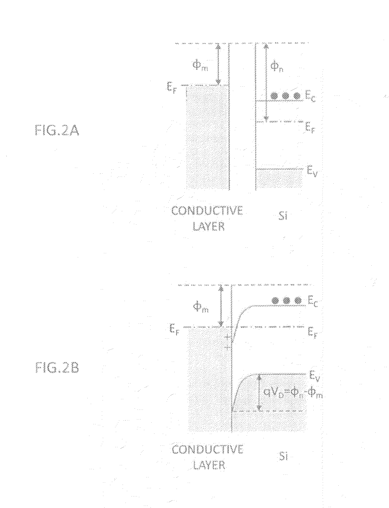
[0049]Single-crystal silicon of n-type having a resistivity of 200 Ωcm produced by a floating zone method was cut to a thickness of 5 mm. To remove a strained layer on the surface of the silicon substrate, etching was performed using a chemical solution obtained by mixing fluorine (a concentration of 50 weight %), nitric acid (a concentration of 70 weight %), and methanol at a volume ratio of 2:5:3. A 500 nm Y film was formed by sputtering as a conductive layer on one surface of the n-type silicon target material obtained as described above. A 500 nm Cr film was also formed as a metal film on the Y film. The Cr film and a backing plate of oxygen-free copper were bonded together by a bonding material containing indium as a main component, to thereby obtain a silicon target for sputtering film formation.

[0050]A 152 mm-square photomask substrate made of synthetic silica was prepared, and a MoSiON film (Mo:Si:O:N=1:4:1:4) having a film thickness of 76 nm was formed on the substrate by D...


PUM

PropertyMeasurementUnit
volume resistivityaaaaaaaaaa
thicknessaaaaaaaaaa
work functionaaaaaaaaaa

Abstract

A silicon target for sputtering film formation which enables formation of a high-quality silicon-containing thin film by inhibiting dust generation during sputtering film formation is provided. An n-type silicon target material 10 and a metallic backing plate 20 are attached to each other via a bonding layer 40. A conductive layer 30 made of a material having a smaller work function than that of the silicon target material 10 is provided on a surface of the silicon target material 10 on the bonding layer 40 side. That is, the silicon target material 10 is attached to the metallic backing plate 20 via the conductive layer 30 and the bonding layer 40. In a case of single-crystal silicon, a work function of n-type silicon is generally 4.05 eV. A work function of a material of the conductive layer 30 needs to be smaller than 4.05 eV.

Description

BACKGROUND OF THE INVENTION[0001]1. Field of the Invention[0002]The present invention relates to a silicon target for sputtering film formation and a method for forming a silicon-containing thin film.[0003]2. Description of the Related Art[0004]Silicon-containing thin films such as a silicon film, a silicon oxide film, a silicon nitride film, and a silicon nitride-oxide film are used in various fields. For example, the silicon-containing thin films are used as an insulator film and a dielectric film in the field of semiconductor devices, as an antireflective film in the field of optical materials, or as a light-shielding film and a phase-shifting film in the field of photomask technology.[0005]A sputtering method using a silicon-containing target material has been widely used to form the silicon-containing thin films for reasons that the method can be performed at low cost, there are relatively few material restrictions therein, and the method is highly controllable.[0006]The silico...

Claims


Application Information

Patent Timeline
Patent Type & Authority Applications(United States)
IPC IPC(8): H01J37/34C23C14/14
CPCC23C14/14H01J37/3426C23C14/0676C23C14/3407C23C14/3414H01L21/0274
Inventor YOSHIKAWA, HIROKIINAZUKI, YUKIOKANEKO, HIDEO
Owner SHIN ETSU CHEM IND CO LTD
Why Eureka
Try Eureka