Touch-sensor-embedded display panel, display device provided therewith, and method for driving touch-sensor-embedded display panel

a display panel and touch sensor technology, applied in the field of touch sensor-embedded display panels, can solve the problems of increasing the power demand for driving the touch panel, increasing the overall weight and thickness of the display panel and touch panel, etc., to reduce the increase of the frame area, reduce the decrease of the aperture ratio, and eliminate the effect of auxiliary capacitan

Active Publication Date: 2014-11-06
SHARP KK
View PDF5 Cites 25 Cited by
  • Summary
  • Abstract
  • Description
  • Claims
  • Application Information

AI Technical Summary

Benefits of technology

[0061]According to the first or the fifteenth aspect of the present embodiment, there is adopted a configuration that only a liquid crystal capacitance is formed as a capacitance for holding a voltage which corresponds to a source signal applied to the image signal line. This eliminates auxiliary capacitances. Therefore, it is no longer necessary for the first substrate which is provided by a TFT substrate for example, to be formed with common electrodes and various other wiring to be connected thererto that are otherwise necessary to form the auxiliary capacitances. This makes it possible to reduce decrease in aperture ratio and to decrease increase in frame area. Also, in a display device which uses a back light, it is now possible to reduce increase in power consumption by the back light since decrease in the aperture ratio is now reduced and therefore it is no longer necessary to set a back light brightness to a higher level in order to ensure a predetermined level of display brightness. Further, the arrangement reduces load at the time of driving the display panel since no use is made for auxiliary capacitances which generally require relatively high level of capacitance value settings, and since the common electrodes are not provided on the first substrate side which is provided by, e.g., a TFT substrate, but are provided only on the second substrate side which is provided by, e.g., a CF substrate. This makes it possible to reduce power consumption. Also, with such a level of saving in power consumption, it is no longer necessary to provide such power saving means as decreasing drive frequency during the display operation, and decreasing the number of integration operations (decreasing the periodic number of burst waveform) performed during the touch detection operation. In other words, it becomes possible to reduce

Problems solved by technology

However, out-cell touch panels have problems that they increase overall weight and thickness of t

Method used


Image

  • Touch-sensor-embedded display panel, display device provided therewith, and method for driving touch-sensor-embedded display panel
  • Touch-sensor-embedded display panel, display device provided therewith, and method for driving touch-sensor-embedded display panel
  • Touch-sensor-embedded display panel, display device provided therewith, and method for driving touch-sensor-embedded display panel

Examples


first embodiment

1. First Embodiment

1.1 Overall Configuration and Operation Outline

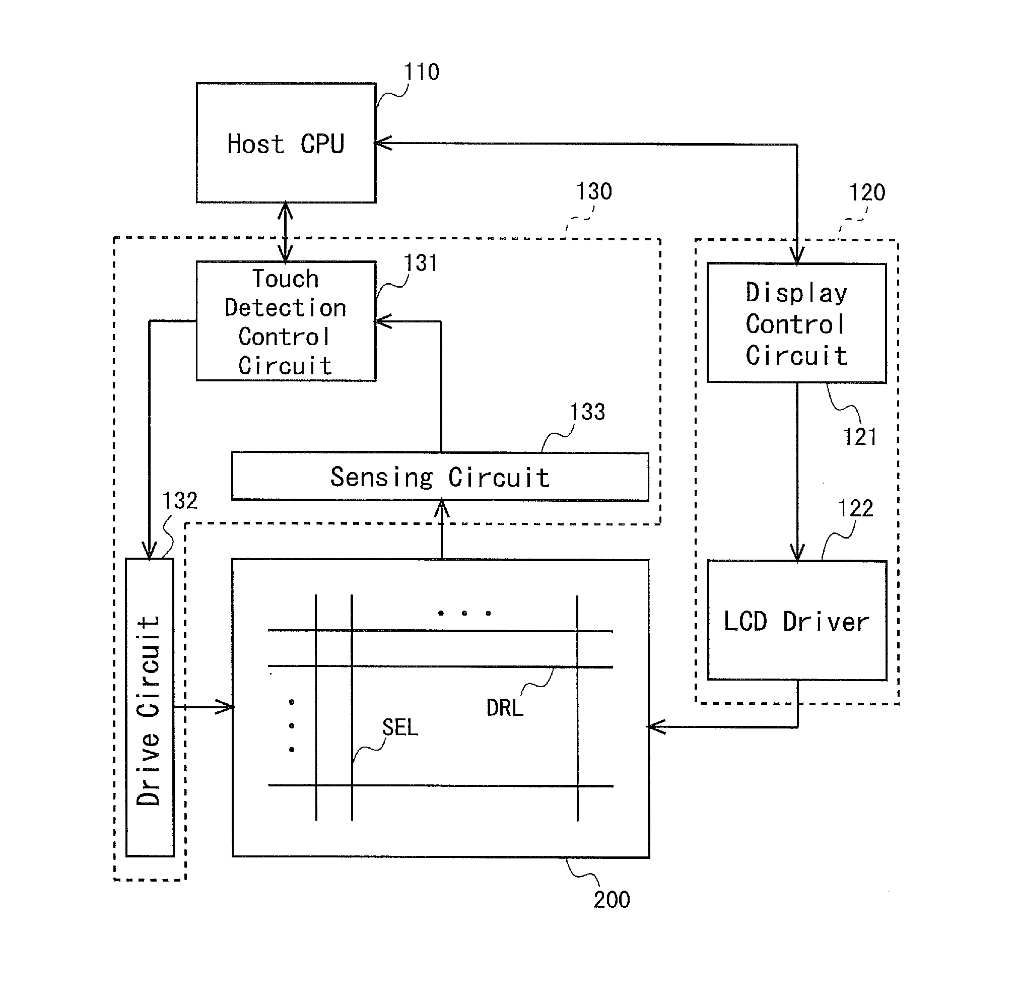
[0094]FIG. 1 is a block diagram which shows an overall configuration of a liquid crystal display device according to a first embodiment of the present invention. This liquid crystal display device not only has image display functions as a liquid crystal display device but also has touch sensor functions. As shown in FIG. 1, the present liquid crystal display device includes: a host CPU 110, a display control unit 120, a touch detection control unit 130, and a touch-sensor-embedded liquid crystal display panel 200 (hereinafter simply called “display panel 200”). The display control unit 120 includes a display control circuit 121 and an LCD driver 122. The touch detection control unit 130 includes a touch detection control circuit 131, a drive circuit 132 and a sensing circuit 133. Though not illustrated in the figure, there is a back light provided behind the display panel 200.

[0095]In the display panel 200, a pluralit...

second embodiment

2. Second Embodiment

2.1 Common-Electrode Pattern

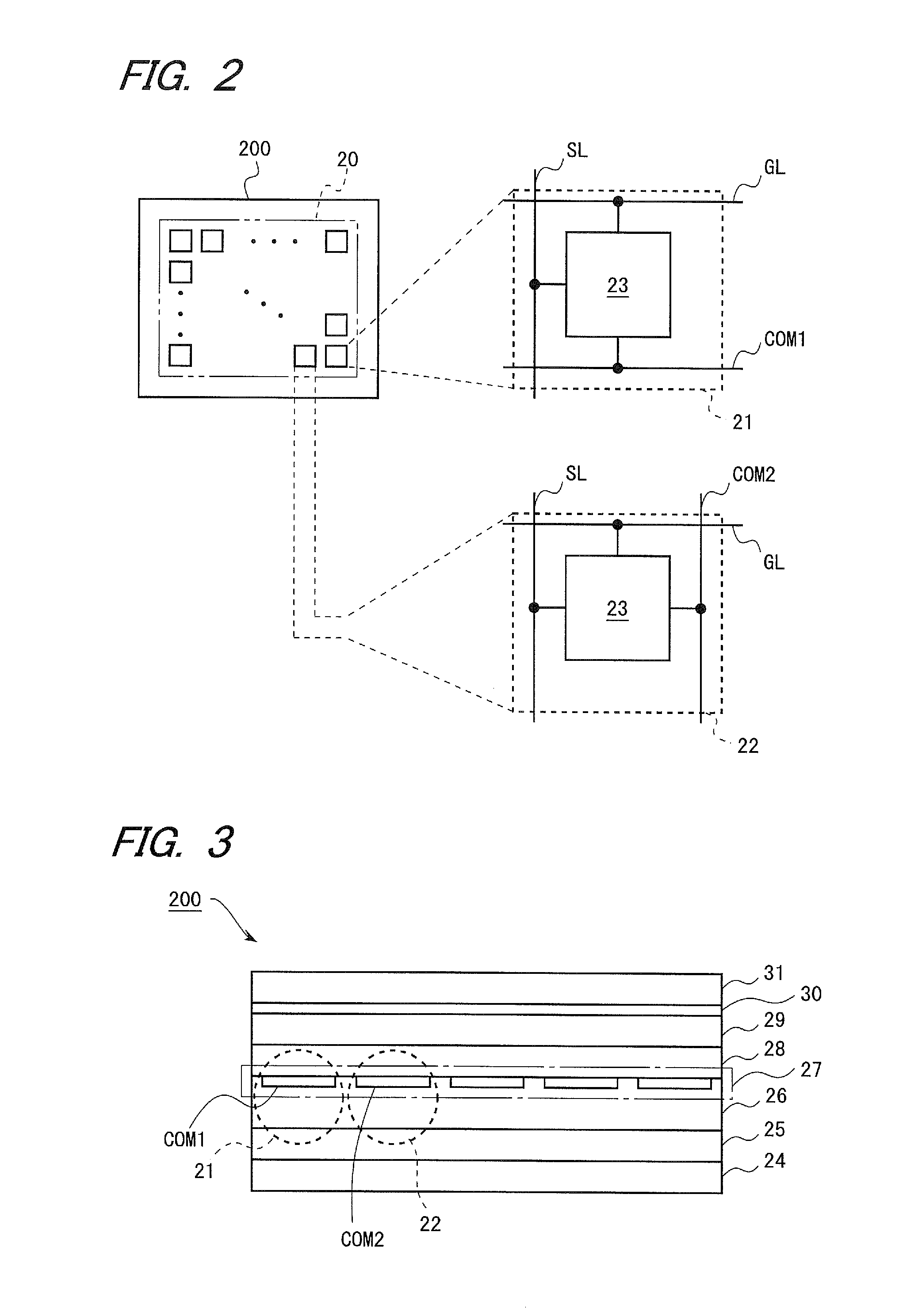
[0131]FIG. 13 is a diagram which shows part of a common-electrode pattern on a CF substrate 28 according to a second embodiment of the present invention. The present embodiment basically share the configuration and other arrangements with the first embodiment except for the common-electrode pattern, so description for those common aspects will not be repeated. As shown in FIG. 13, in the present embodiment, a plurality of substantially diamond-shaped regions 41 arranged in a Y direction are electrically connected to each other to provide sensing lines SEL. In the present embodiment, these substantially diamond-shaped regions 41 which form the sensing lines SEL will be called “sensing segment”. Also, a plurality of a plurality of substantially diamond-shaped 42 arranged in an X direction are electrically connected to each other to provide driving lines DRL. In the present embodiment, these diamond-shaped regions 42 which form the drivin...

third embodiment

3. Third Embodiment

3.1 Conventional Art

[0134]Before moving to a third embodiment of the present invention, description will be made for conventional art which is relevant to the third embodiment. FIG. 15 is an equivalent-circuit diagram which shows a pixel configuration in a conventional liquid crystal display device which utilizes a multiple pixel structure. The pixel structure shown in FIG. 15 is disclosed in Non-Patent Document 1 for example. The term “multiple pixel structure” refers to a pixel structure in which a pixel is divided into a plurality (typically, two) sub-pixels in order to eliminate visual-angle dependency of gamma characteristic in VA and other types of liquid crystal display panels. The term “a pixel” used here actually refers to “a sub-pixel” according to the first embodiment, and the term “sub-pixel” used here refers to what is obtained by dividing the “sub-pixel” according to the first embodiment. For the sake of expedience, however, description will be made ...


PUM


Abstract

There is provided a touch-sensor-embedded display panel with reduced decrease in aperture ratio and reduced increase in frame area, with lowered power consumption and improved operation performance.
A driving pixel (21) is constituted by: a thin film transistor (T1); a pixel electrode (Epix1); a driving common electrode (COM1); and a liquid crystal capacitance (Clc1) which is formed between the pixel electrode (Epix1) and the driving common electrode (COM1). A sensing pixel (22) is constituted by a thin film transistor (T2), a pixel electrode (Epix2), a sensing common electrode (COM2), and a liquid crystal capacitance (Clc2) which is formed between the pixel electrode (Epix2) and the sensing common electrode (COM2). Neither the driving pixel (21) nor the sensing pixel (22) include an auxiliary capacitance. The thin film transistors (T1, T2) have their channel layers formed of IGZO.

Description

TECHNICAL FIELD[0001]The present invention relates to touch-sensor-embedded display panels, and more specifically to a display panel incorporating a capacitive touch sensor, a display device provided therewith, and a method for driving the display panel.BACKGROUND ART[0002]Touch panels have been a focus of attention as an input device in operating computer systems and the like. In a capacitance touch panel for example, a position of a target object such as an operator's finger or a pen is detected on the basis of electrostatic capacitance changes between a driving line and a sensing line. Conventionally, such a touch panel as described is placed on a display panel provided by a liquid crystal display panel for example. The touch panel provided on the display panel as described above is called “out-cell touch panel” for example.[0003]However, out-cell touch panels have problems that they increase overall weight and thickness of the display panel and touch panel, and that they increas...

Claims


Application Information

Patent Timeline
IPC IPC(8): G06F3/044
CPCG06F3/044G09G3/3648G02F1/13338G06F3/0412G06F3/042G06F3/0445
Inventor SUGITA, YASUHIROKIDA, KAZUTOSHITANAKA, KOHHEI
Owner SHARP KK
Why Eureka
Try Eureka