

Electronic device
- Summary
- Abstract
- Description
- Claims
- Application Information
AI Technical Summary
Benefits of technology
Problems solved by technology
Method used
Image

Examples
Embodiment Construction
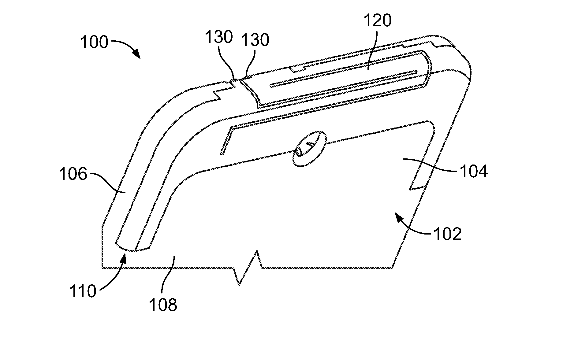
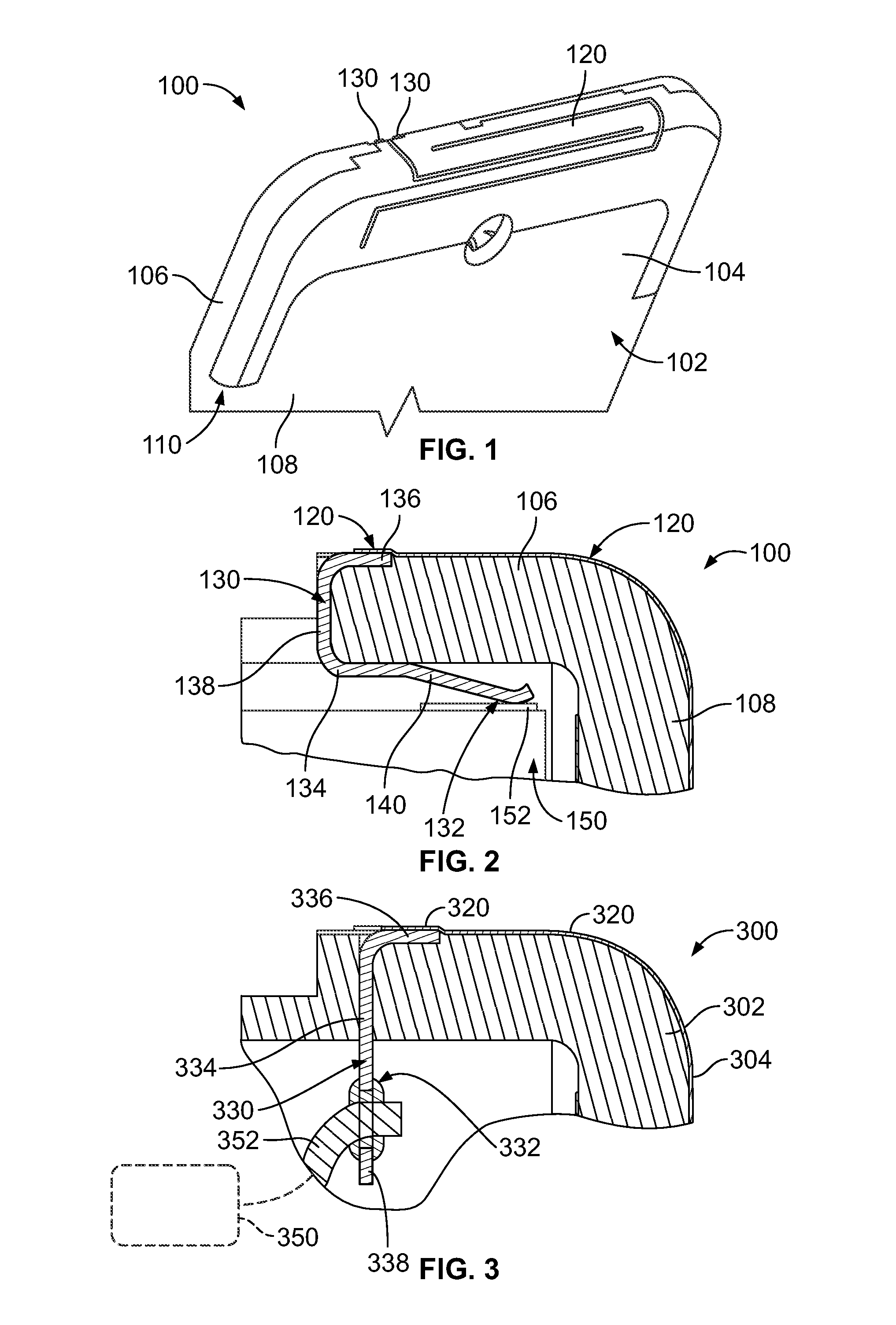
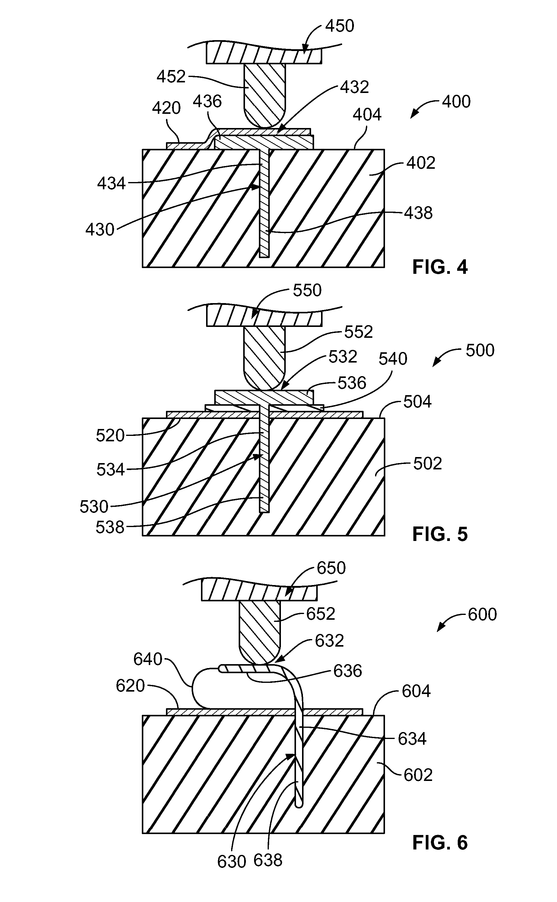
[0015]Embodiments described herein may provide an electronic device having improved wear life of conductive circuits of the electronic device. Embodiments described herein may provide a printed conductive ink trace on a surface of a dielectric substrate. Embodiments described herein may provide a separate conductive interposer electrically coupled to the printed conducted ink trace having a contact interface for a contact or other conductive component to be electrically connected to the conductive circuit defined by the printed conductive ink trace. The conductive interposer between the conductive circuit and the other contact eliminates mating to and unmating from the conductive circuit by the other contact, which reduces wear on the conductive circuit. For example, movement between the contact and the conductive circuit, such as during mating and unmating, may cause scraping of the printed conductive ink trace, which can damage or destroy the conductive circuit.
[0016]FIG. 1 illust...
PUM
| Property | Measurement | Unit |
|---|---|---|
| Flexibility | aaaaa | aaaaa |
| Electrical conductor | aaaaa | aaaaa |
Abstract
Description
Claims
Application Information