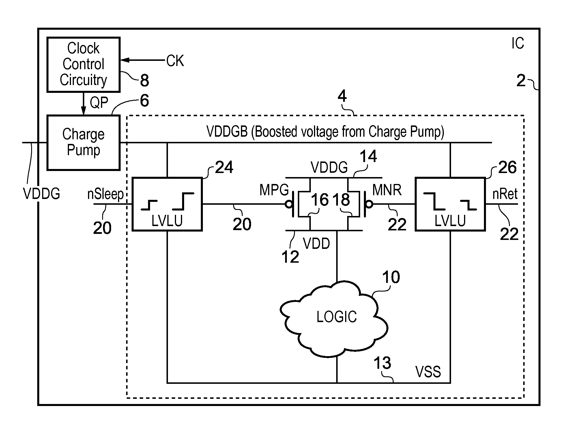
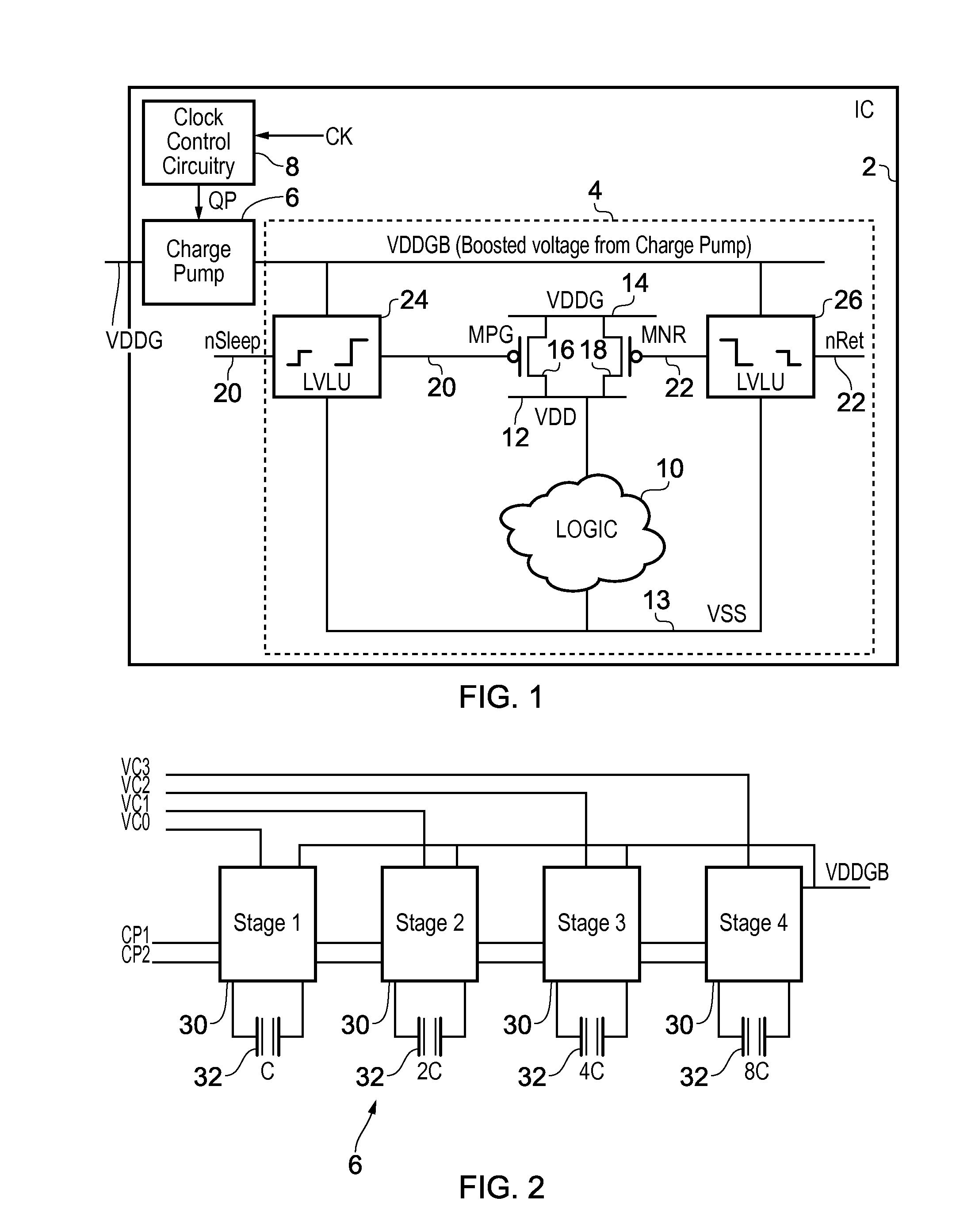
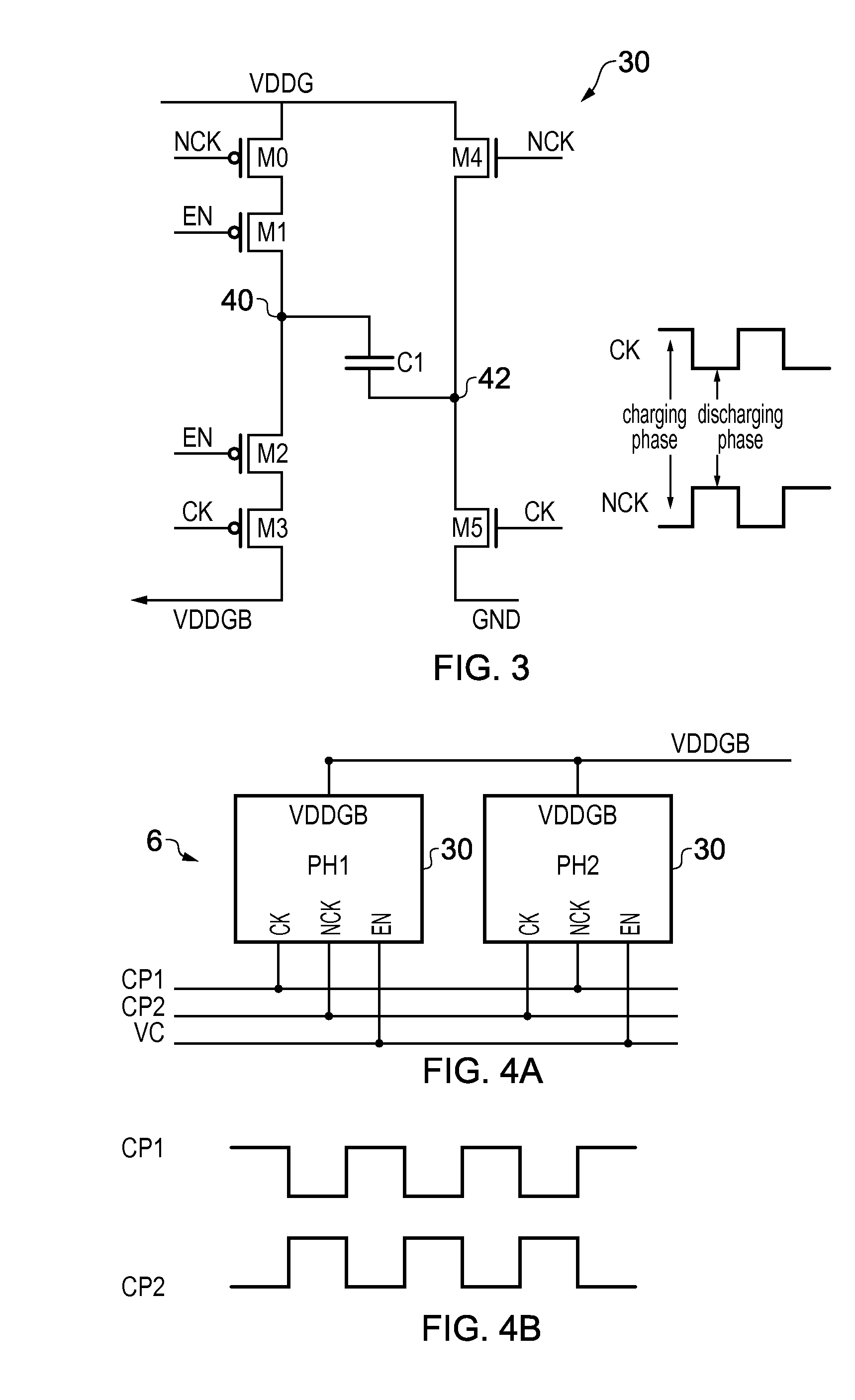
[0011]Voltage generating circuitry generates an on-chip voltage from a supply voltage in response to clock pulses of a voltage generation clock signal. The on-chip voltage is supplied to a circuit block within the integrated circuit. Clock control circuitry is provided to control transmission of the clock pulses of the voltage generation clock signal to the voltage generating circuitry. By reducing the frequency with which clock pulses are transmitted to the voltage generating circuitry, the clock control circuitry can reduce the power consumed by the voltage generating circuitry, but less frequent pulses may cause the level of the on-chip voltage to drop. The circuit block may require a given voltage level to operate correctly, and so the clock control circuitry may compare the on-chip voltage with a reference voltage to determine whether a clock pulse should be transmitted to the voltage generation circuitry. The clock control circuitry may suppress transmission of clock pulses of the voltage generation clock signal if the on-chip voltage rises beyond the desired value, in order to save power. If the voltage drops too low, then a clock pulse can be sent to the voltage generation circuitry to trigger further generation of the on-chip voltage. In this way, the average level of the on-chip voltage can be controlled to a desired target level.
[0013]To address this problem, the present technique provides the clock control circuitry with the ability to digitally tune the comparison of the on-chip voltage with a reference voltage. A digital offset value is provided to the clock control circuitry which identifies, from a binary numeric value, an offset for the reference voltage. The clock control circuitry suppresses transmission of clock pulses to the voltage generating circuitry if the on-chip voltage is greater than the sum of the reference voltage and an offset identified by the digital offset value. By supplying different digital offset values, different offsets of the reference voltage can be selected so as to vary the level of the on-chip voltage at which transmission of clock pulses is suppressed or permitted. By providing a digitally tunable offset, any existing voltage within the integrated circuit can be used as the reference voltage, and there is no need for an analogue voltage generator for generating a variable reference voltage. Eliminating the need for an analogue reference voltage generator reduces the power consumed by the integrated circuit and significantly eases implementation.
[0014]Another advantage of the present technique is that the clock control circuitry can adapt to different load conditions of the circuit block in a power efficient way. Sometimes the circuit block may have a greater load than at other times (depending on the extent to which the circuit block is active). At times when the circuit load is low, it can be a waste of energy to continue sending many clock pulses to the voltage generating circuitry. In a previous proposal, this problem was addressed by providing a ring oscillator to artificially load the voltage generating circuitry, but this is not power efficient as the oscillator may consume a significant amount of power. In the present technique, the voltage comparison used to control the density of clock pulses supplied to the voltage generating circuitry can detect changes in the on-chip voltage caused by varying circuit loads and adjust the rate at which clock pulses are transmitted accordingly to save power.
[0023]At least some of the pulling transistors in the second circuitry may pass different drive currents in response to the same level of reference voltage. For example, the transistors may have different sizes, different semiconductor doping conditions, or some other difference in configuration which causes them to pass different drive currents in response to the same level of reference voltage. While it would be possible to provide a number of identically configured pulling transistors, providing differently configured pulling transistors increases the granularity with which the offset can be changed since different combinations of active pulling transistors will pass different total drive currents. For example, if the different drive currents are in ratios of powers of two then the total drive current can be approximately proportional to the binary value of the digital offset value. For example, if the switching transistors corresponding to pulling transistors with drive currents in ratios 16, 8, 4, 2, 1 are controlled in response to bits [4:0] of the digital offset value respectively, then 5 transistors can provide 32 relatively evenly distributed levels of drive currents and hence 32 different offsets to the reference voltage. In contrast, if all the pulling transistors provide the same drive current then 5 transistors could only provide 5 different levels of offset (corresponding to 1, 2, 3, 4 and 5 transistors being active), since different permutations of active / non-active transistors would correspond to the same total drive current.
[0044]The technique described above where a digitally adjusted offset tunes a clocked comparison between a voltage and a reference voltage can also be used for applications other than controlling voltage generation. The clocked comparator may have comparing circuitry which compares a first voltage against a reference voltage with offset, and tuning circuitry for adjusting the comparing circuitry to vary the offset in response to the digital offset value. This enables the clocked comparator to tune the level against which the first voltage is compared without requiring an analogue component such as a reference voltage generator or digital-to-analogue converter, which would increase power consumption and circuit complexity.


