Variable temperature solders for multi-chip module packaging and repackaging

a multi-chip module and variable temperature technology, applied in the field of semiconductor processing, can solve the problems of affecting the post-fabrication fault of one chip, destroying one chip without impact, and a lot of semiconductor chips are more prone to post-fabrication faults than others

Active Publication Date: 2014-11-27
ADVANCED MICRO DEVICES INC
View PDF7 Cites 10 Cited by
  • Summary
  • Abstract
  • Description
  • Claims
  • Application Information

AI Technical Summary

Problems solved by technology

Stacked semiconductor chip devices present a host of design and integration challenges for scientists and engineers.
Common problems include providing adequate electrical interfaces between the stacked semiconductor chips themselves and between the individual chips and some type of circuit board, such as a motherboard or semiconductor chip package substrate, to which the semiconductor chips are mounted.
Still another technical challenge associated with stacked semiconductor chips is testing.
If, for example, the first semiconductor chip mounted to a circuit board is revealed to be defective only after several other semiconductor chips are stacked thereon, then all of the material processing steps and the materials associated with the later-mounted chips may have been wasted.
To non-destructively remove one chip without impacting the viability of the solder bumps associated with a remaining chip is a technical challenge.
Furthermore, some types of semiconductor chips may be more prone to post-fabrication faults than others.

Method used


Image

  • Variable temperature solders for multi-chip module packaging and repackaging
  • Variable temperature solders for multi-chip module packaging and repackaging
  • Variable temperature solders for multi-chip module packaging and repackaging

Examples


Embodiment Construction

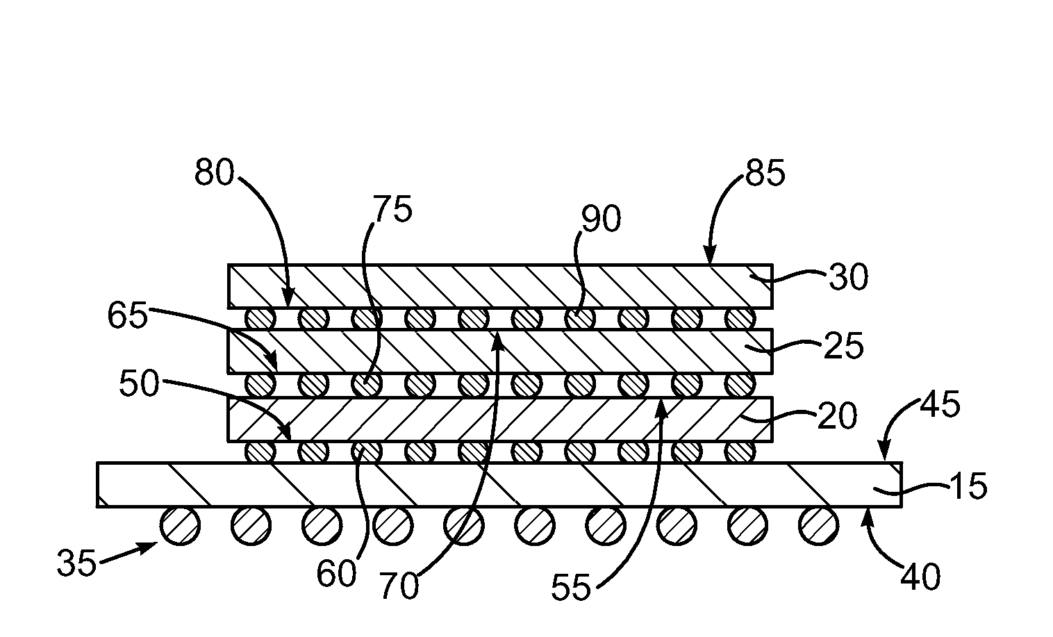
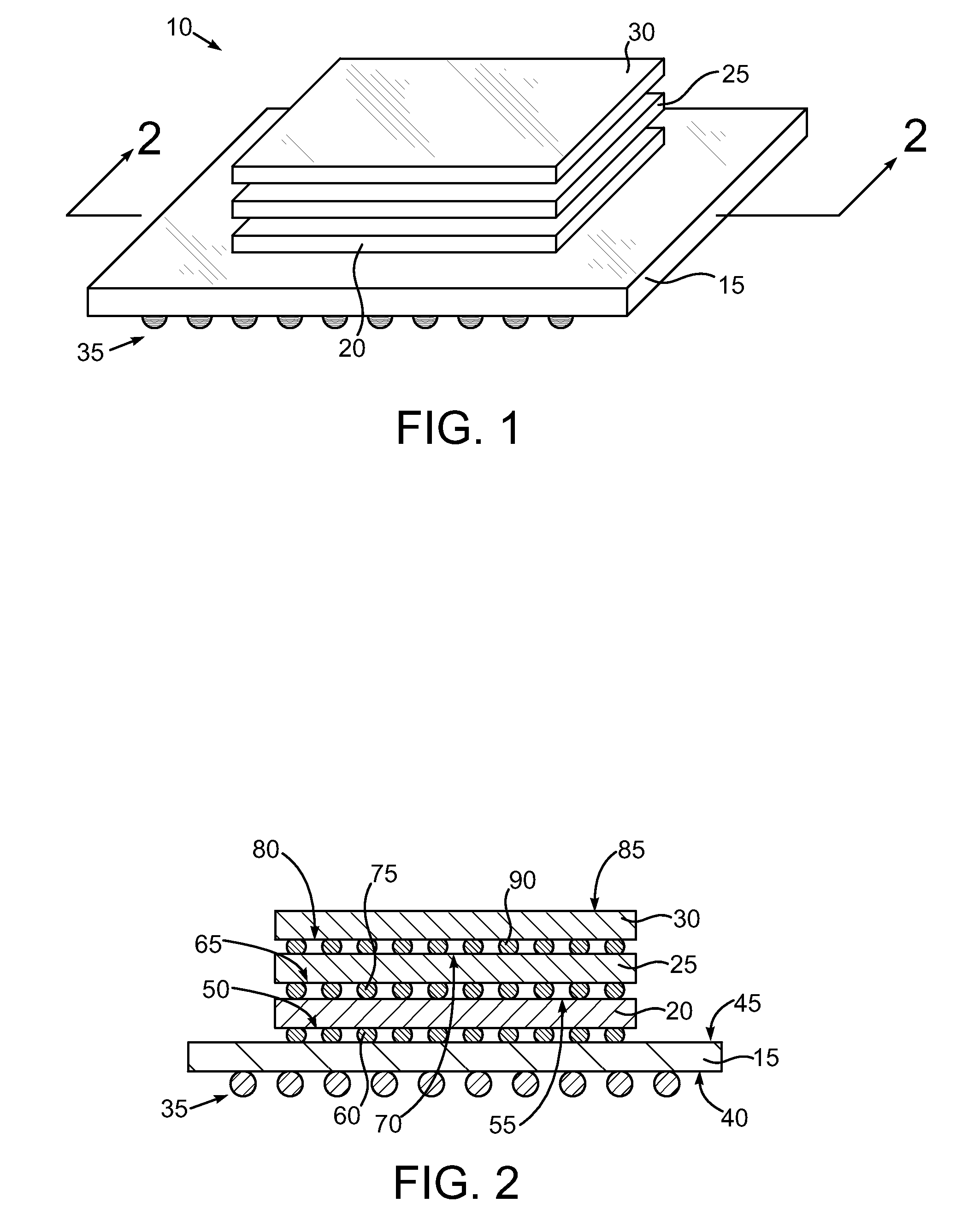
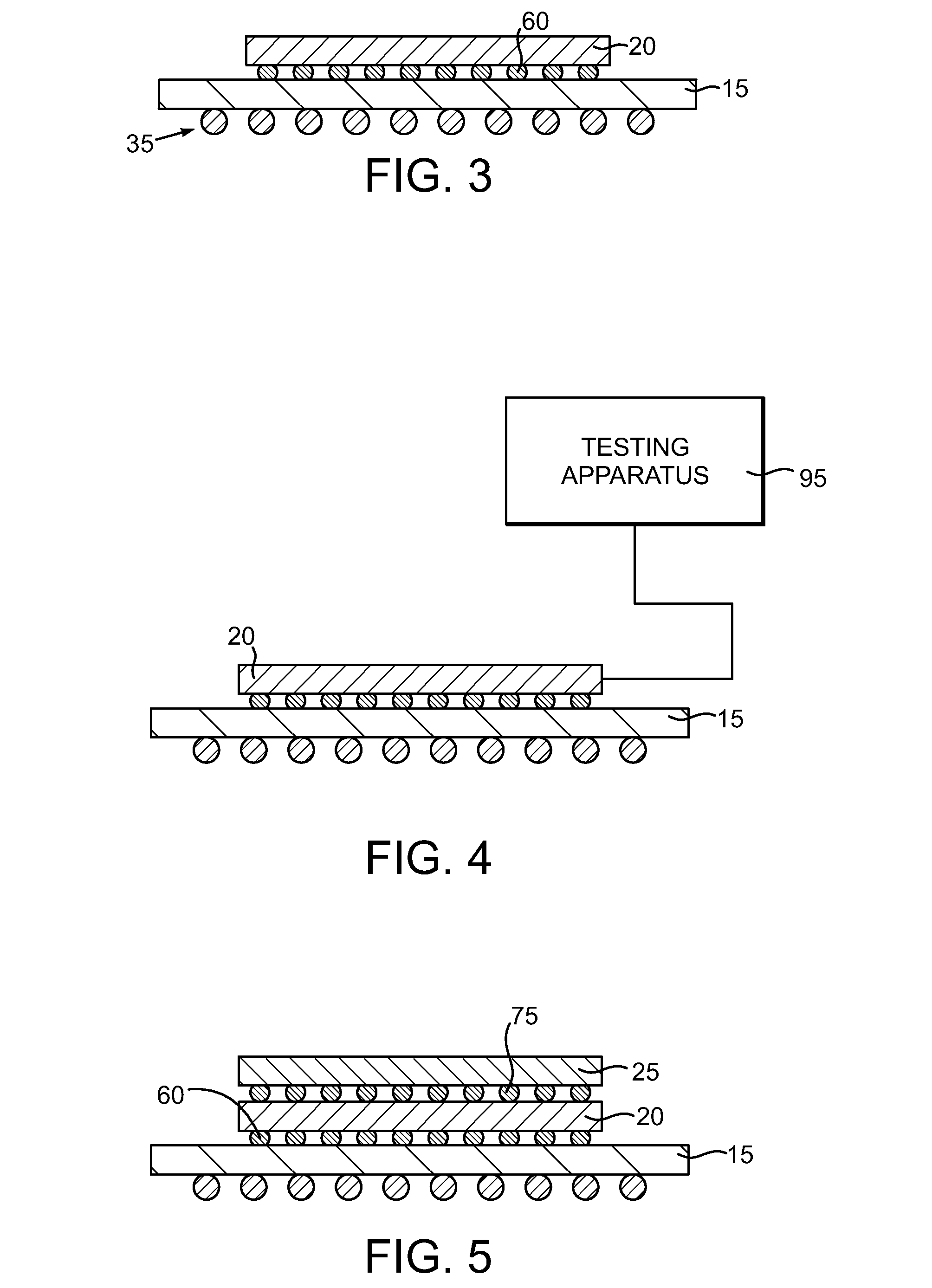
[0008]In accordance with one aspect of an embodiment of the present invention, a method of manufacturing is provided that includes coupling a first plurality of solder interconnect structures to a first semiconductor chip. The first solder interconnect structures have a first melting point. The first semiconductor chip may be tested. If the first semiconductor chip passes the testing, then a second semiconductor chip is coupled to the first semiconductor chip using a second plurality of solder interconnect structures that have a second melting point lower than the first melting point.

[0009]In accordance with another aspect of an embodiment of the present invention, a method of manufacturing is provided that includes coupling a first semiconductor chip to a substrate using a first plurality of solder interconnect structures. The first solder interconnect structures have a first melting point. A second semiconductor chip is coupled to the first semiconductor chip using a second plural...


PUM

PropertyMeasurementUnit
melting pointaaaaaaaaaa
conductiveaaaaaaaaaa

Abstract

Various methods of mounting semiconductor chips on a substrate are disclosed. In one aspect, a method of manufacturing is provided that includes coupling a first plurality of solder interconnect structures to a first semiconductor chip. The first solder interconnect structures have a first melting point. The first semiconductor chip may be tested. If the first semiconductor chip passes the testing, then a second semiconductor chip is coupled to the first semiconductor chip using a second plurality of solder interconnect structures that have a second melting point lower than the first melting point.

Description

BACKGROUND OF THE INVENTION[0001]1. Field of the Invention[0002]This invention relates generally to semiconductor processing, and more particularly to methods and apparatus for stacking multiple semiconductor devices and packaging the same.[0003]2. Description of the Related Art[0004]Stacked semiconductor chip devices present a host of design and integration challenges for scientists and engineers. Common problems include providing adequate electrical interfaces between the stacked semiconductor chips themselves and between the individual chips and some type of circuit board, such as a motherboard or semiconductor chip package substrate, to which the semiconductor chips are mounted. Still another technical challenge associated with stacked semiconductor chips is testing.[0005]A process flow to transform bare semiconductor wafers into collections of semiconductor chips and then mount those semiconductor chips on an interposer or circuit board involves a large number of individual ste...

Claims


Application Information

Patent Timeline
Patent Type & Authority Applications(United States)
IPC IPC(8): H01L23/00
CPCH01L24/81H01L2224/175H01L2224/81801H01L24/17H01L22/14H01L22/20H01L24/13H01L24/16H01L24/98H01L25/0657H01L25/50H01L2224/13023H01L2224/13082H01L2224/131H01L2224/13109H01L2224/13111H01L2224/13116H01L2224/13139H01L2224/13144H01L2224/13147H01L2224/13164H01L2224/13169H01L2224/1601H01L2224/16145H01L2224/16225H01L2224/17181H01L2224/17505H01L2224/81815H01L2225/06513H01L2225/06517H01L2225/06565H01L2924/01322H01L2924/12042H01L2924/15311H01L2924/014H01L2924/01047H01L2924/01029H01L2924/01082H01L2924/0105H01L2924/00014H01L2924/00012H01L2924/00
Inventor EPPES, DAVID H.
Owner ADVANCED MICRO DEVICES INC
Why Eureka
Try Eureka