Impedance matching device

a technology of impedance matching and matching device, which is applied in the direction of light sources, electric lighting sources, electric discharge tubes, etc., can solve the problems of reducing the size affecting the cost reduction, and complicated impedance matching devices, so as to save time and cost, the size and manufacturing cost of the impedance matching device can be reduced.

Active Publication Date: 2014-12-04
DAIHEN CORP
View PDF10 Cites 14 Cited by
  • Summary
  • Abstract
  • Description
  • Claims
  • Application Information

AI Technical Summary

Benefits of technology

[0021]With the above arrangements, there is no need to provide a detector or circuit at the output port for detecting the p-p value Vpp of the high-frequency voltage. Thus, the size and

Problems solved by technology

This arrangement has the following disadvantages:(1) The structure adjacent to the output port of the impedance matching device is complicated.(2) The impedance matching device cannot be reduced in size.(3) To detec

Method used


Image

  • Impedance matching device
  • Impedance matching device
  • Impedance matching device

Examples


Embodiment Construction

[0028]Preferred embodiments of the present invention are described below with reference to the accompanying drawings.

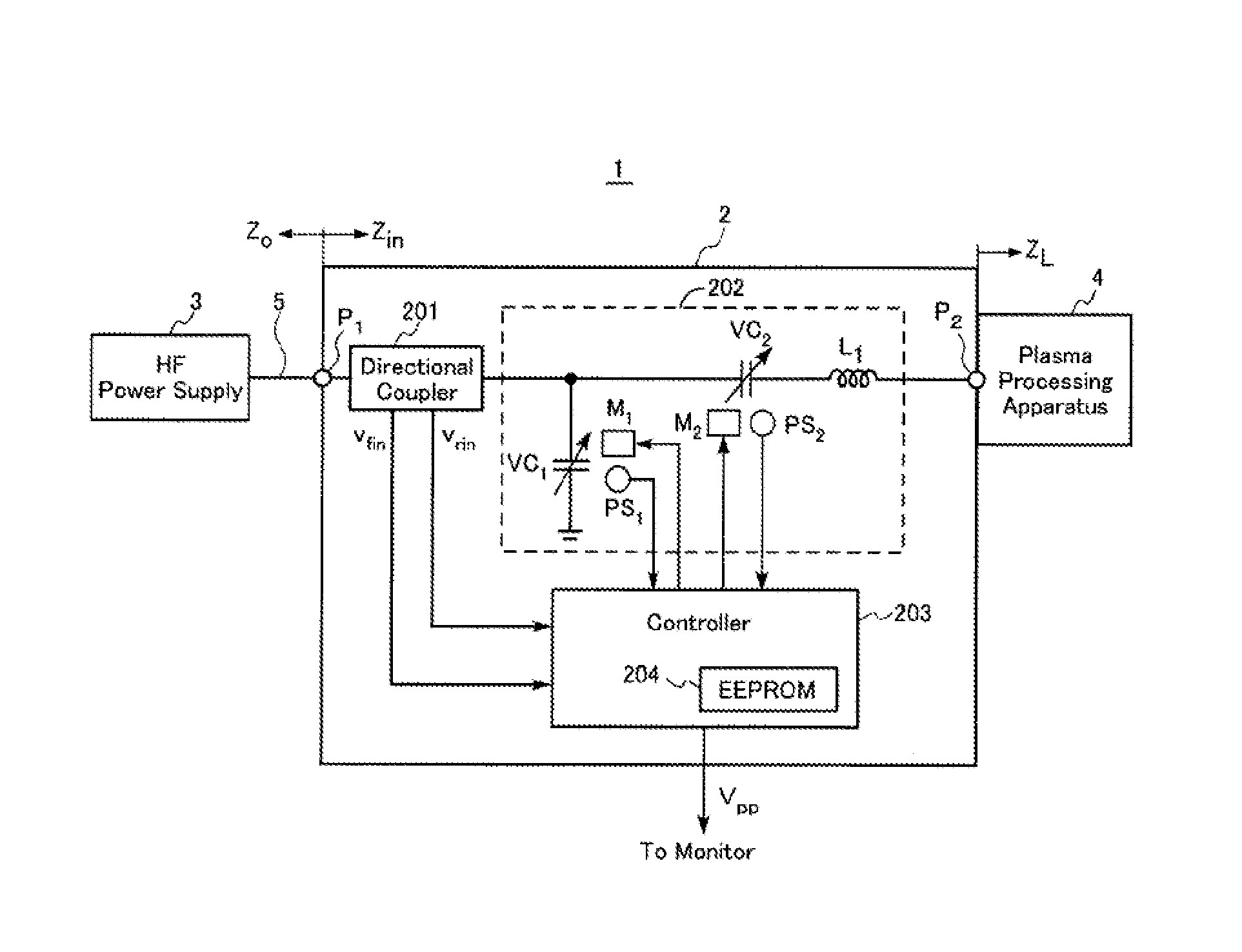
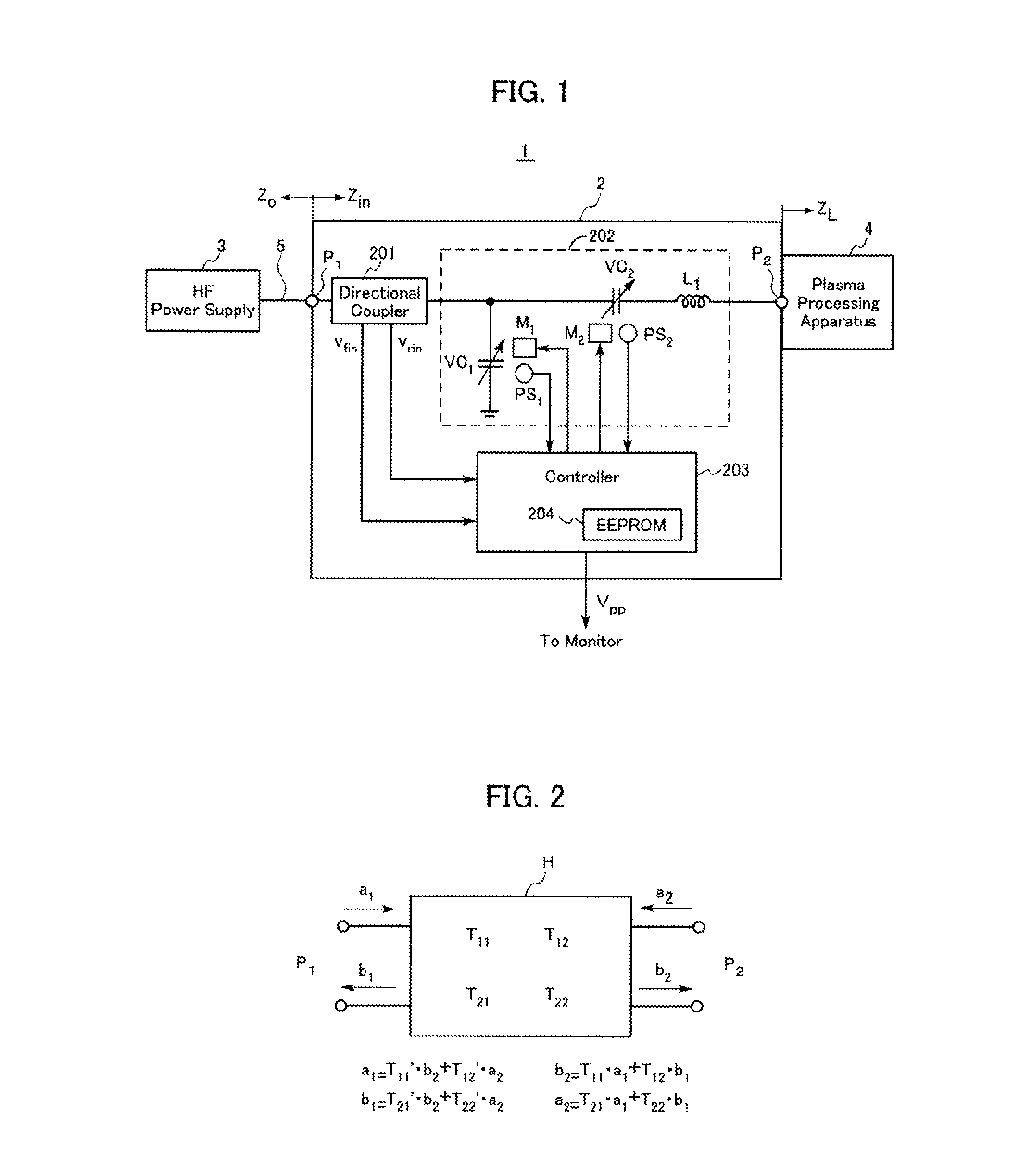
[0029]FIG. 1 shows the schematic structure of a plasma processing system to which an impedance matching device according to an embodiment of the present invention is applied.

[0030]The plasma processing system 1 shown in FIG. 1 includes an impedance matching device 2 according to the present invention, a high-frequency power supply 3, and a plasma processing apparatus 4. The high-frequency power supply 3 is connected to the input port P1 of the impedance matching device 2 by a transmission cable 5 (e.g. a coaxial cable having a characteristic impedance Zc of 50Ω). The plasma processing apparatus 4 is directly connected to the output port P2 of the impedance matching device 2.

[0031]The plasma processing apparatus 4 is an apparatus for performing e.g. thin film formation or etching by using plasma to an object such as a semiconductor wafer or a liquid crystal substrate. ...


PUM


Abstract

An impedance matching device includes an input port connected to a high-frequency power supply, an output port connected to a load, an impedance variable circuit, a T-parameter memory for storing sets of T-parameters in a manner such that each of the sets of T-parameters is related to a corresponding one of adjustable impedance values of the device, an input voltage detector for detecting a forward wave voltage and a reflected wave voltage at the input port, and a p-p value calculator for computation of a p-p value of a high-frequency voltage at the output port. The computation of the p-p value of the high-frequency voltage is performed by using the forward wave voltage and the reflected wave voltage detected at the input port and also using one set of the T-parameters stored in the T-parameter memory.

Description

BACKGROUND OF THE INVENTION[0001]1. Field of the Invention[0002]The present invention relates to an impedance matching device for performing impedance matching between a high-frequency power supply and a load.[0003]2. Description of the Related Art[0004]A plasma processing system for forming a thin semiconductor film or etching is conventionally known. In such a plasma processing system, high-frequency power is supplied from a high-frequency power supply to a plasma processing apparatus to generate plasma in the plasma processing apparatus. To efficiently supply high-frequency power from the high-frequency power supply to the plasma processing apparatus during the plasma processing, an impedance matching device is provided between the high-frequency power supply and the plasma processing apparatus. The impedance matching device operates to match the impedance of the high-frequency power supply and that of the plasma processing apparatus.[0005]In the plasma processing system, the pea...

Claims


Application Information

Patent Timeline
IPC IPC(8): H01J37/32
CPCH01J37/32009H03H7/40H01J37/32183
Inventor MATSUNO, DAISUKE
Owner DAIHEN CORP
Why Eureka
Try Eureka