Micromechanical structure and coresponding manufacturing method

Inactive Publication Date: 2014-12-04
ROBERT BOSCH GMBH
View PDF8 Cites 0 Cited by
  • Summary
  • Abstract
  • Description
  • Claims
  • Application Information

AI Technical Summary

Benefits of technology

The patent describes a method for producing a structure that can absorb light using standard microstructuring methods, such as photolithography and reactive ion etching. This structure can be used in a process for producing micromirrors, for example, without needing additional steps. The structure has trenches and webs that help with absorption. It can also be covered with layers that increase reflectance without affecting absorption. The main advantage of this method is that it allows for precise placement of light-absorbing regions in the initial steps of production.

Problems solved by technology

This is because light that is reflected by these surfaces commonly produces undesired blooms that in the case of the micromirror can have a disturbing appearance as artifacts in the produced image, and can greatly reduce the contrast that can be achieved.
A problem with this type of surface treatment is that its quality is a function both of the wavelength and of the angle of incidence of the light.
However, even in this way it is not possible to achieve an optimal treatment for a large wavelength range and for arbitrary angles of incidence.
These cover the overall silicon surface like grass, and cause it to appear black, because they drastically reduce the reflectance for visible light.
The fine, exposed silicon tips can however easily be destroyed in subsequent process steps.

Method used


Image

  • Micromechanical structure and coresponding manufacturing method
  • Micromechanical structure and coresponding manufacturing method
  • Micromechanical structure and coresponding manufacturing method

Examples


Embodiment Construction

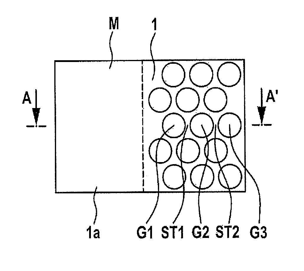
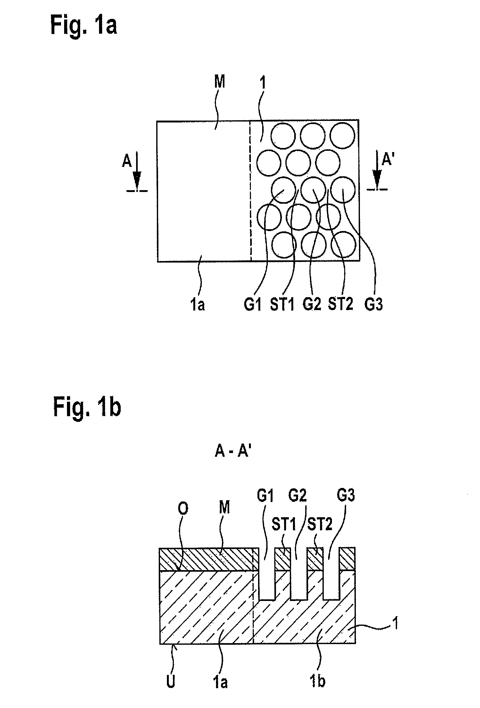
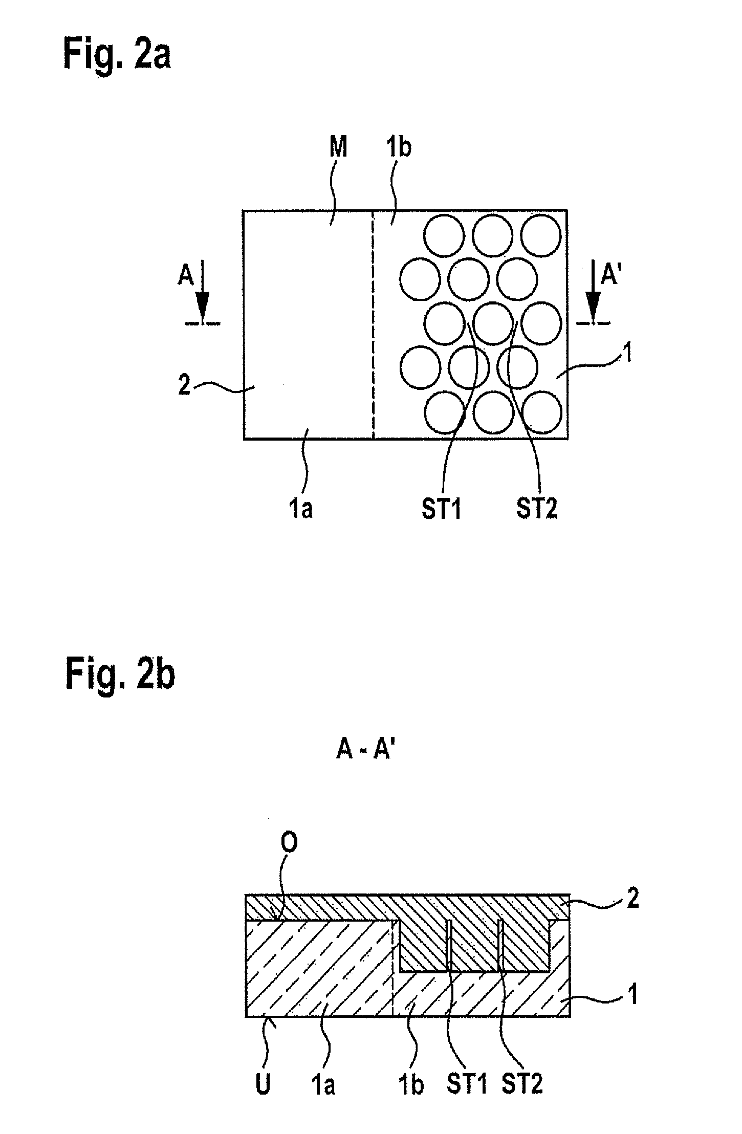
[0026]In the Figures, identical reference characters designate identical or functionally identical elements.

[0027]FIGS. 1a), b) and FIGS. 2a), b) are schematic representations of a micromechanical structure according to a first specific embodiment of the present invention, FIGS. 1a) and 2a) in a top view and FIGS. 1b) and 2b) in vertical cross-section along line A-A′ in FIG. 1a) or, respectively, 2a).

[0028]In FIGS. 1a), b), reference character 1 designates a silicon substrate having an upper side O and a lower side U on which there is deposited an etching mask M, e.g. of silicon nitride, as trench etching mask. Using a known trench etching process, through the presence of corresponding holes in etching mask M holes G1, G2, G3, etc., with web regions ST1, ST2, etc. positioned between them, are etched in a region 1b of the silicon substrate, the holes structuring region 1b to form a network-type substrate region made of silicon. Etching mask M is sealed in region 1a of the silicon sub...


PUM


Abstract

A micromechanical structure includes a substrate having an upper side and a lower side, the substrate having a first region and a second region adjacent thereto, the upper side being fashioned in the first region as a mirror region that reflects light. In the second region on the upper side of the substrate, a network-type structure and / or a web-type structure is fashioned, such that the second region is essentially non-light-reflective.

Description

BACKGROUND OF THE INVENTION[0001]1. Field of the Invention[0002]The present invention relates to a micromechanical structure and to a corresponding production method.[0003]2. Description of the Related Art[0004]Although it is applicable to arbitrary optical materials, the present invention and the problem on which it is based are explained on the basis of silicon.[0005]Given the use of silicon as a base material for micromechanical components in optical applications, e.g. for micromirrors for projection applications, as known from published international patent application document WO 2009 / 019086 A1, the reflectance and absorbance of the surface play a large role.[0006]A high reflectance is required on the actual mirror surface of a micromirror. For visible light, given perpendicular incidence, silicon has a degree of reflection of only about 35%. In order to increase the degree of reflection on such mirror surfaces to a higher level, thin metallic layers can be applied, e.g. of sil...

Claims


Application Information

Patent Timeline
IPC IPC(8): G02B26/08
CPCG02B26/0833B81B3/0083B81B2201/042B81B2203/0353G02B5/003
Inventor SCHORR, NICOLASHEUCK, FRIEDJOFTRAUTMANN, ACHIMBAADER, JOHANNESROHLFING, FRANZISKAPINTER, STEFANSTRAUB, RAINER
Owner ROBERT BOSCH GMBH
Why Eureka
Try Eureka