Substrate processing apparatus, method of manufacturing semiconductor device, and non-transitory computer-readable recording medium

a processing apparatus and substrate technology, applied in the direction of coatings, chemical vapor deposition coatings, electric discharge tubes, etc., can solve the problems of insufficient improvement of in-plane uniformity or in-plane uniformity in substrate processing, and the productivity of substrate processing may be decreased, so as to improve the inter-plane uniformity and in-plane uniformity of substrate processing without reducing the productivity of substrate processing

Active Publication Date: 2014-12-04
KOKUSA ELECTRIC CO LTD
View PDF10 Cites 67 Cited by
  • Summary
  • Abstract
  • Description
  • Claims
  • Application Information

AI Technical Summary

Benefits of technology

[0125]According to this embodiment, one or a plurality of effects to be described will be obtained.
[0126](a) According to this embodiment, in step 3, the H2 gas is supplied into the process chamber 201 using the nozzle 233a (first nozzle) including at least the plurality of gas supply holes 248a that are provided from the top to the bottom so as to correspond to a substrate arrangement region in which the plurality of wafers 200 are arranged. Also, at this time, the O2 gas is supplied into the process chamber 201 using the nozzles 233d and 233e (second nozzle) including at least one of the gas supply holes 248d and 248e that is provided at only the top and the bottom so as to correspond to only the wafers 200 arranged at the top and the bottom out of the plurality of wafers 200. Accordingly, it is possible to uniformize a concentration distribution of an oxidizing species (atomic oxygen) generated by reacting the O2 gas and the H2 gas in an entire wafer arrangement region, in particular, in a wafer arrangement direction. As a result, it is possible to improve inter-plane uniformity and in-plane uniformity of the film thickness of the SiO film formed on the plurality of wafers 200. Also, since there is no need to reduce the number of batch-processed wafers 200, it is possible to prevent productivity decrease of substrate processing.
[0127]Also, as in this embodiment, in step 3, the H2 gas is supplied into the process chamber 201 using the nozzle 233a including at least the same number of gas supply holes 248a as the plurality of wafers 200 that are provided from the top to the bottom so as to correspond one-to-one to the plurality of wafers 200. Also, at this time, by supplying the O2 gas into the process chamber 201 using the nozzles 233d and 233e including at least one of the gas supply holes 248d and 248e that are provided at only the top and the bottom so as to correspond one-to-one to the wafers 200 arranged at the top and the bottom out of the plurality of wafers 200, it is easy to obtain the above effects.
[0128]Here, for reference, a case of forming a SiO film using a conventional substrate processing apparatus will be described with reference to FIG. 6.
[0129]A vertical processing furnace of the conventional substrate processing apparatus illustrated in FIG. 6 includes a process chamber configured to accommodate a plurality of wafers arranged in a vertical direction in a horizontal posture, a nozzle configured to supply the HCDS gas and the H2 gas into the process chamber, and a nozzle configured to supply O2 gas into the process chamber. These two nozzles are provided at positions separated by a predetermined distance, so as to extend along a stacking direction of the wafers are arranged, along an outer circumference of the wafer. In addition, at sides of these two nozzles, at least the same number of gas supply holes as the plurality of wafers are provided so as to correspond one-to-one to the plurality of wafers accommodated in the process chamber. The plurality of wafers arranged at intervals in a vertical direction in a horizontal posture are accommodated in the process chamber. Then, a process of supplying the HCDS gas into the process chamber, and a process of supplying the O2 gas and the H2 gas into the process chamber 200 under heated atmosphere having a pressure lower than an atmospheric pressure are alternately performed a predetermined number of times, with a purge process of removing a residual gas in the process chamber interposed therebetween. Thereby, the SiO film may be formed on the wafer.
[0130]An in-plane film thickness distribution of the SiO film formed using the vertical processing furnace illustrated in FIG. 6 was examined. The result showed that a film thickness of the SiO film decreases in the vicinity of the center of the wafer and increases in the vicinity of the outer circumference. That is, it was found that the in-plane film thickness distribution has a conical shape (concave). This phenomenon is called a loading effect in a plane within the wafer (loading effect) (hereinafter simply referred to as an in-plane LE). As a cause of the in-plane LE, a case in which a processing gas such as the HCDS gas, the O2 gas, and the H2 gas is consumed in the vicinity of the outer circumference of the wafer and is not sufficiently supplied in the vicinity of the center of the wafer, that is, insufficient supply of the processing gas, may be exemplified. Also, insufficient removal (insufficient purge) of the residual gas in the above purge process may be exemplified as one of the factors. When the residual gas is insufficiently removed, a plurality of different processing gases are mixed in the process chamber, which causes a gas phase reaction. As a result, the film thickness of the SiO film may increase in the vicinity of the outer circumference of the wafer.

Problems solved by technology

However, depending on types of the processing gas, even when the gas is supplied using the multi-hole nozzle, the inter-plane uniformity or the in-plane uniformity in substrate processing may not be sufficiently improved.
Specifically, when a hydrogen-containing gas and an oxygen-containing gas are used as the processing gas, even if the gas is supplied using the multi-hole nozzle, the in-plane uniformity or the inter-plane uniformity in the substrate processing may not be sufficiently improved.
However, in this case, the productivity of substrate processing may be decreased.

Method used


Image

  • Substrate processing apparatus, method of manufacturing semiconductor device, and non-transitory computer-readable recording medium
  • Substrate processing apparatus, method of manufacturing semiconductor device, and non-transitory computer-readable recording medium
  • Substrate processing apparatus, method of manufacturing semiconductor device, and non-transitory computer-readable recording medium

Examples


example 1

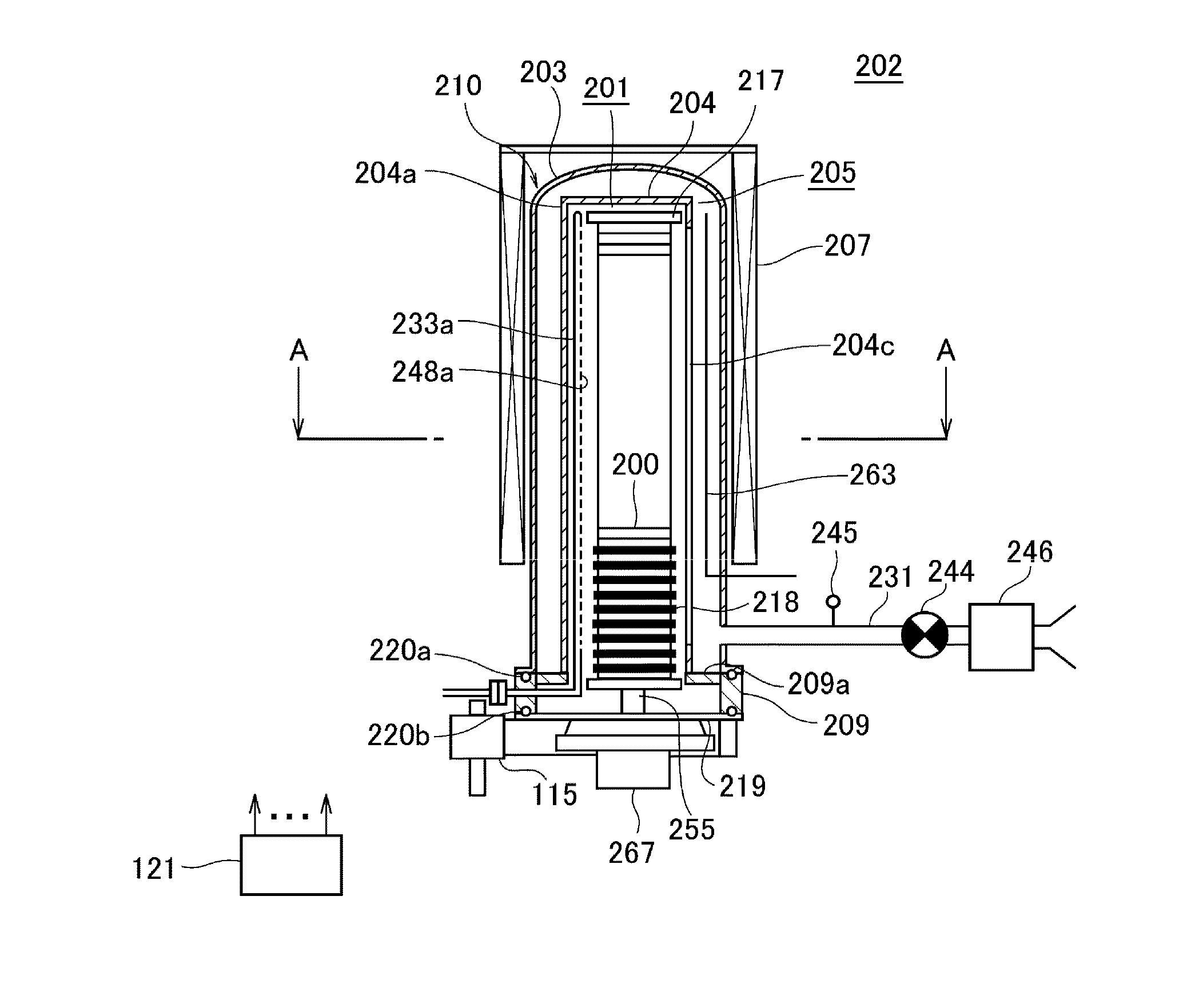
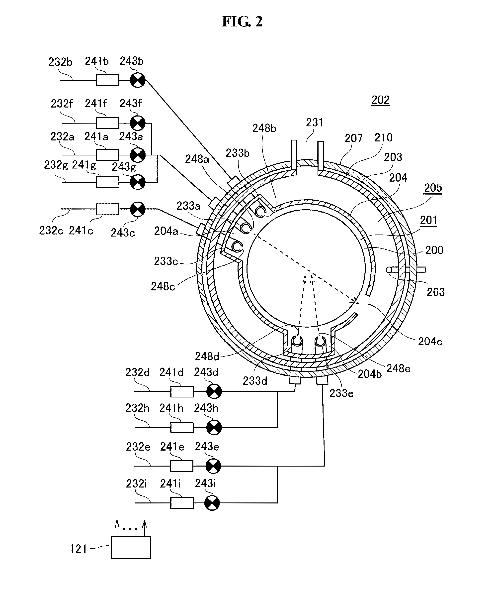
[0179]As example 1, the SiO film was formed on the plurality of wafers by the film-forming sequence illustrated in FIG. SA using the substrate processing apparatus in the above embodiment. The HCDS gas was used as the source gas, the O2 gas was used as the oxygen-containing gas, and the H2 gas was used as the hydrogen-containing gas. Supply of the O2 gas was performed using the nozzles 233d and 233e of the type illustrated in FIG. 4B. During film formation, the boat, that is, the wafer, was rotated. The processing conditions were set to predetermined values within the processing condition ranges described in the above embodiment. In addition, as comparative example 1, the SiO film was formed on the plurality of wafers using the vertical processing furnace illustrated in FIG. 6. Gas types, film-forming sequences, and processing conditions used in comparative example 1 were the same as in example 1.

[0180]FIG. 10A is a graph showing inter-plane film thickness uniformity of the SiO film...

example 2

[0181]As example 2, the SiO film is formed on the plurality of wafers by the film-forming sequence illustrated in FIG. 5A using the substrate processing apparatus in the above embodiment. Gas types, film-forming sequences, and processing conditions used in example 2 were the same as in example 1. Supply of the O2 gas was performed using the nozzles 233d and 233e of the type illustrated in FIG. 4B. Supply of the HCDS gas and supply of the H2 gas were performed using the nozzle 233b. During film formation, the boat, that is, the wafer, was not rotated.

[0182]Also, as comparative example 2, the SiO film was formed on the plurality of wafers by the film-forming sequence illustrated in FIG. SA using the substrate processing apparatus in the above embodiment. Gas types, film-forming sequences, and processing conditions used in comparative example 2 were the same as in example 2. Supply of the O2 gas was performed using the nozzle 233c, and supply of the HCDS gas and supply of the H2 gas we...


PUM

PropertyMeasurementUnit
pressureaaaaaaaaaa
pressureaaaaaaaaaa
timeaaaaaaaaaa

Abstract

There is provided a substrate processing apparatus including: a process chamber configured to accommodate and process a plurality of substrates arranged with intervals therebetween; a first nozzle extending along a stacking direction of the substrates and configured to supply a hydrogen-containing gas into the process chamber; and a second nozzle extending along the stacking direction of the substrates and configured to supply an oxygen-containing gas into the process chamber, wherein the first nozzle includes a plurality of first gas supply holes disposed in a region extending from an upper portion to a lower portion of the first nozzle corresponding to a substrate arrangement region where the substrates are arranged, and the second nozzle includes a plurality of second gas supply holes disposed at an upper portion and a lower portion of the second nozzle to correspond to upper substrates and lower substrates of the substrates.

Description

CROSS-REFERENCE TO RELATED PATENT APPLICATION[0001]This U.S. non-provisional patent application claims priority under 35 U.S.C. §119 of Japanese Patent Application No. 2013-117280 filed on Jun. 3, 2013 in the Japanese Patent Office, the entire contents of which are hereby incorporated by reference.BACKGROUND OF THE INVENTION[0002]1. Field of the Invention[0003]The present invention relates to a substrate processing apparatus processing a substrate, a method of manufacturing a semiconductor device, and a non-transitory computer-readable recording medium.[0004]2. Description of the Related Art[0005]As a process among manufacturing processes of a semiconductor device, a substrate processing process in which a processing gas is supplied into a process chamber accommodating a plurality of substrates arranged at intervals and the plurality of substrates are batch-processed is performed.[0006]In the above substrate processing process, a method of supplying a processing gas into a process c...

Claims


Application Information

Patent Timeline
Patent Type & Authority Applications(United States)
IPC IPC(8): H01L21/02
CPCH01L21/02532H01L21/0262C23C16/308C23C16/402C23C16/403C23C16/405C23C16/45523C23C16/45534H01L21/67109H01J37/32449
Inventor TAKAGI, KOSUKEAKAE, NAONORITERASAKI, MASATOOHNO, MIKIO
Owner KOKUSA ELECTRIC CO LTD
Why Eureka
Try Eureka