Fault detection apparatus

a technology of fault detection and fault detection, which is applied in the direction of transmission monitoring, testing circuits, instruments, etc., can solve the problem of difficulty in visually verifying the state of mounted solder balls

Inactive Publication Date: 2014-12-18
TOSHIBA MEMORY CORP
View PDF20 Cites 153 Cited by
  • Summary
  • Abstract
  • Description
  • Claims
  • Application Information

AI Technical Summary

Benefits of technology

[0008]There is provided a fault detection apparatus which can detect a fault of a test apparatus with a high accuracy.

Problems solved by technology

In the printed circuit board (the mounting substrate), it is difficult to visually confirm the state of the mounted solder balls.

Method used


Image

  • Fault detection apparatus
  • Fault detection apparatus
  • Fault detection apparatus

Examples


first embodiment

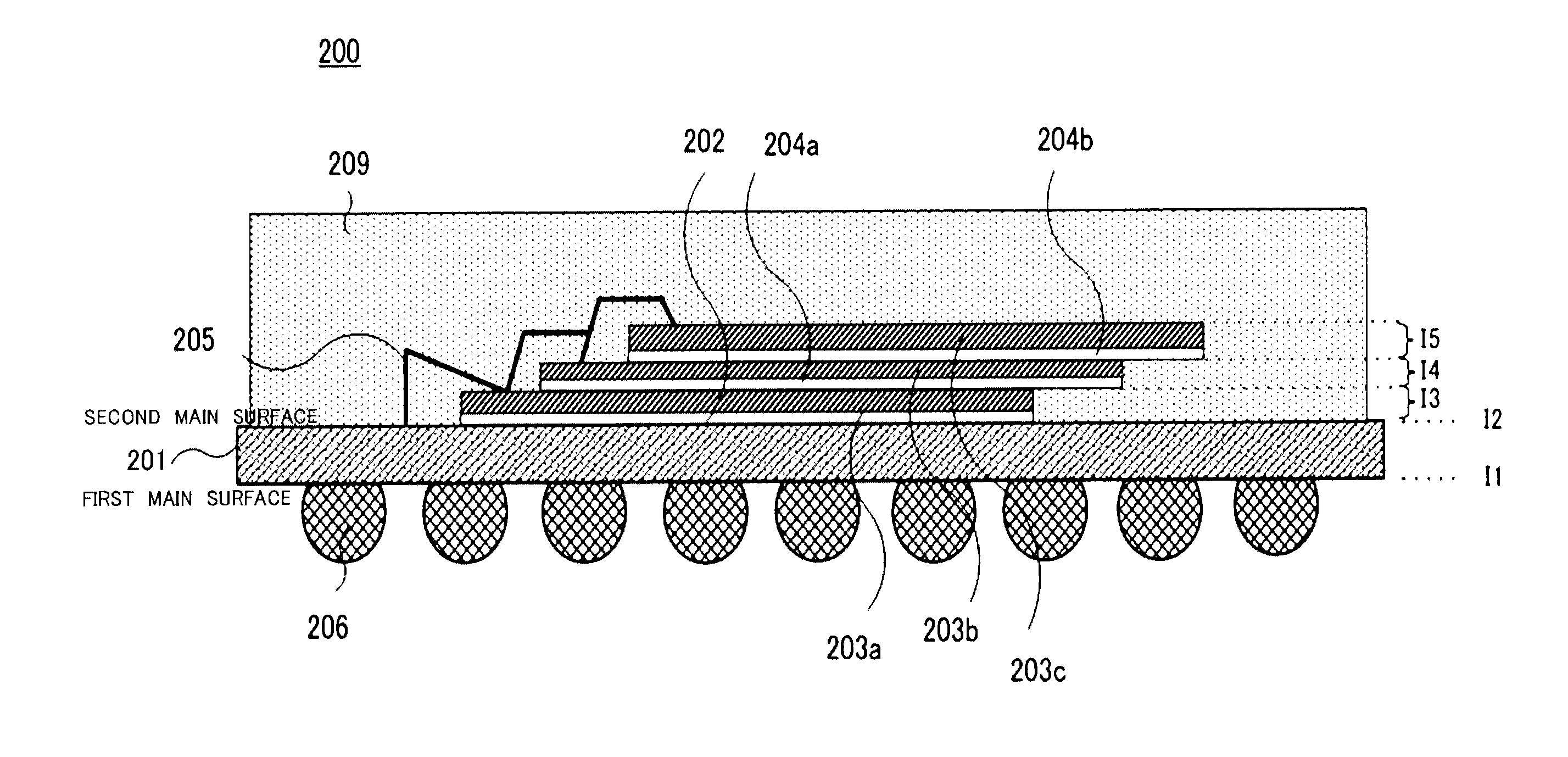
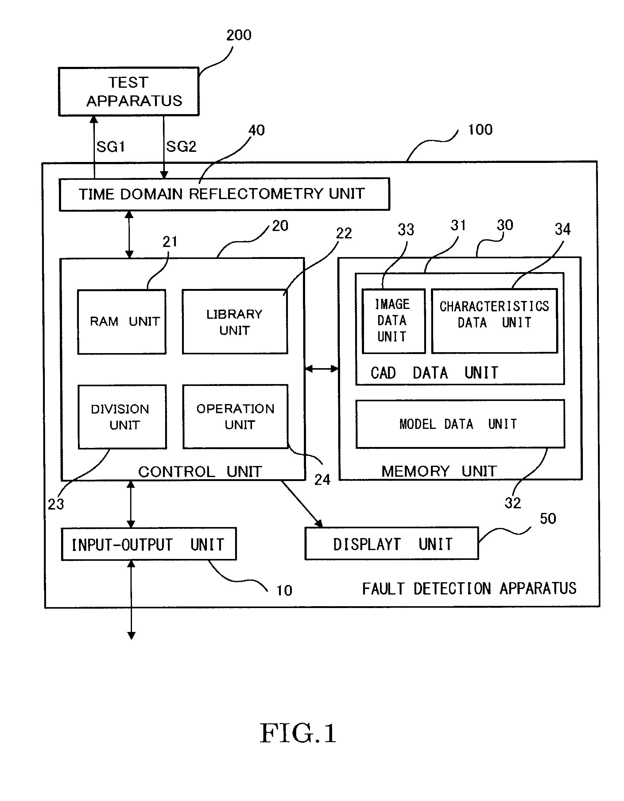
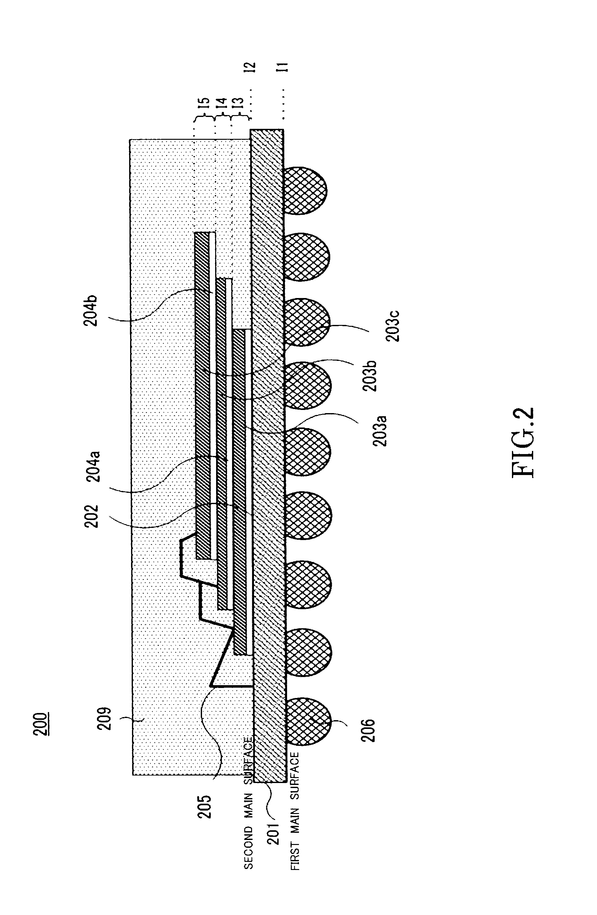
[0026]A fault detection apparatus of a first embodiment will be described with reference to FIG. 1. FIG. 1 is a block diagram illustrating a test apparatus and fault detection apparatus of the embodiment. As illustrated in FIG. 1, a fault detection apparatus 100 and a test apparatus 200 are provided. Herein, the description will be made using a BCA semiconductor apparatus as an example of the test apparatus 200, but the invention is not limited to the configuration, and any apparatus may be employed as long as a plurality of electronic components are electrically connected in the apparatus. For example, there can be exemplified an apparatus such as an LGA semiconductor apparatus which is provided with a ball terminal as an external terminal, stacked with semiconductor chips and sealed with resin, and an SSD card or an SD card in which NAND flash memory chips are stacked, or the like.

[0027]Before describing the fault detection apparatus of the embodiment, the test apparatus will be d...

second embodiment

[0133]A fault detection apparatus of a second embodiment will be described with reference to FIG. 13. FIG. 13 is a diagram illustrating a table relating to the model data which is stored in the memory unit of the fault detection apparatus.

[0134]In the fault detection apparatus of the second embodiment, the model data of the memory unit 30 is differently configured from that of the fault detection apparatus of the first embodiment. The other configurations are the same, and thus only the different portions will be described.

[0135]The memory unit 30 of the fault detection apparatus of the embodiment also stores the model data. Herein, the model data is data (for example, function data) which is obtained by modeling a conductivity characteristic of a pulse wave for each component or portion. The model data is used for specifying a fault in a component or a portion based on data output from the time domain reflectometry unit 40 to be described below, the image data, and the characterist...


PUM


Abstract

A fault detection apparatus according to an embodiment is provided with a measurement unit, a memory unit, a control unit, and a display unit. The measurement unit measures a first time period taken until a reflection signal reflected on a fault of a test apparatus is received after a first signal is transmitted to the test apparatus. The memory unit includes a CAD data unit having CAD data of the test apparatus, and a model data unit to store model data indicating a relation between the first time period and a predicted conduction distance of the first signal according to the CAD data. The control unit calculates a range of a test object selected in the test apparatus based on the CAD data, calculates the predicted conduction distance from the first time period based on the model data, and specifies a position of a fault of the test apparatus which is separated by the predicted conduction distance from the measurement unit in the range of the test object. The display unit displays the position of the fault in the CAD data.

Description

CROSS REFERENCE TO RELATED APPLICATION[0001]This application is based upon and claims the benefit of priority from the prior Japanese Patent Application No. 2012-045742, filed on Mar. 1, 2012, the entire contents of which are incorporated herein by reference.TECHNICAL FIELD[0002]Embodiments described herein relate to a fault detection apparatus which detects a fault using time domain reflectometry (TDR), for example.BACKGROUND ART[0003]In a process of manufacturing an electronic apparatus which mounts electronic components on a mounting substrate, when the electronic components are mounted on the mounting substrate, connection portions on the mounting substrate and connection portions of the electronic components are connected by solder. The connection portions connected by solder are subjected to a test for checking whether a short circuit or an open circuit occurs.[0004]As an example of a semiconductor apparatus, there is a BGA semiconductor apparatus. In the ball grid array, the ...

Claims


Application Information

Patent Timeline
Patent Type & Authority Applications(United States)
IPC IPC(8): G01R31/28
CPCG01R31/2851G01R31/2853G16Z99/00G01R31/71G01R31/11G06F17/40H04B3/46G01D21/00G01R27/16G01R31/08H04B17/00H04B17/309
Inventor SETO, MOTOSHIMURAKAMI, HIROAKI
Owner TOSHIBA MEMORY CORP
Why Eureka
Try Eureka