Imaging element, imaging apparatus, its control method, and control program

Active Publication Date: 2015-01-01
CANON KK
View PDF6 Cites 13 Cited by
  • Summary
  • Abstract
  • Description
  • Claims
  • Application Information

AI Technical Summary

Benefits of technology

[0010]It is, therefore, an aspect of the invention to provide an imaging element

Problems solved by technology

As illustrated in FIG. 7, when the image for AF evaluation is picked up, since a frame rate is set to be higher than the live view image pickup period, a thinning-out rate in the read-out of the imaging element is high and a deterioration in image quality cannot be avoided.
However, in Japanese Patent Application Laid-Open No. 2009-89105, since the image signal (that is, charges) is read out from the imaging element on a pixel unit basis, not only it takes a time to transfer the charges but also a transfer data amount increases, thereby increasing electric power consumption.
Furt

Method used


Image

  • Imaging element, imaging apparatus, its control method, and control program
  • Imaging element, imaging apparatus, its control method, and control program
  • Imaging element, imaging apparatus, its control method, and control program

Examples


Example

First Embodiment

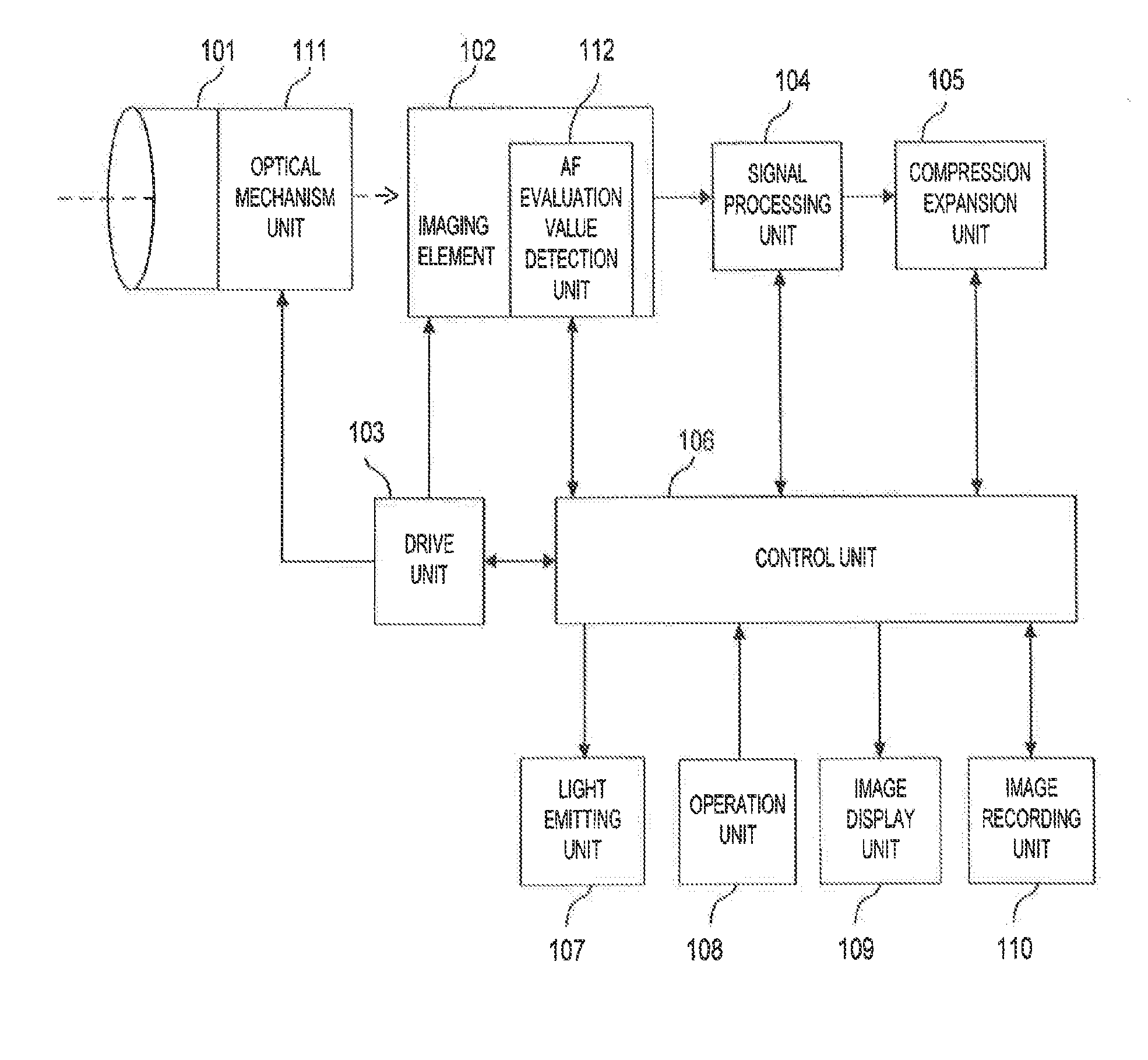
[0033]FIG. 1 is a block diagram illustrating a construction of an imaging apparatus having an imaging element according to the first embodiment of the invention. The illustrated imaging apparatus is applied to, for example, a digital still camera with a moving image function or a video camera.

[0034]In the diagram, an imaging apparatus 100 has an optical barrel 101, an imaging element 102, a drive unit 103, a signal processing unit 104, a compression expansion unit 105, a control unit 106, a light emitting unit 107, an operation unit 108, an image display unit 109, and an image recording unit 110.

[0035]The optical barrel 101 has a lens unit (not shown; hereinbelow, simply called a lens) serving as a photographing optical system and an optical mechanism unit 111. The lens converges (that is, focuses) light (optical image) from an object onto the imaging element 102. Although not shown, the optical mechanism unit 111 has an AF mechanism, a zoom driving mechanism, a mech...

Example

Second Embodiment

[0089]Subsequently, an imaging apparatus having an imaging element according to the second embodiment of the invention will be described. Since a construction of the imaging apparatus according to the second embodiment is similar to that of the camera illustrated in FIG. 1, its description is omitted here. A construction of the imaging element 102 differs from that in the first embodiment (FIG. 2B). The present embodiment will be described hereinbelow with respect to an example of a still image photographing at the time of the photometry operation with a light emitting unit such as a strobe apparatus.

[0090]FIG. 6 is a block diagram illustrating the construction of the imaging element according to the present embodiment. In FIG. 6, substantially the same component elements as those in the imaging element illustrated in FIGS. 2A and 2B are designated by the same reference numerals and their description is omitted here.

[0091]In the imaging element 102 illustrated in FI...

Example

Third Embodiment

[0102]Subsequently, the third embodiment of the invention will be described with reference to FIGS. 8A to 11B.

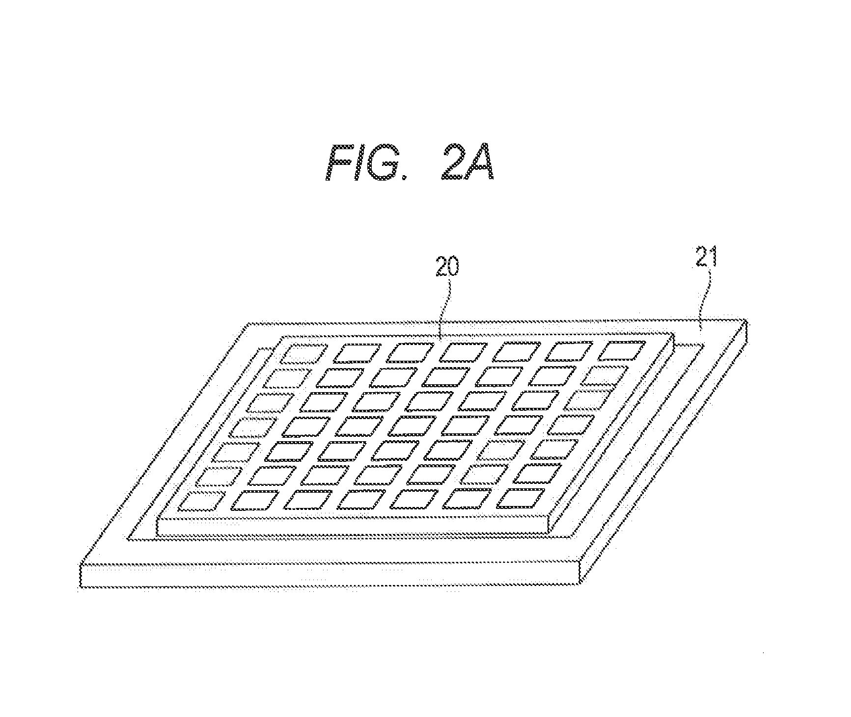
[0103]The imaging element illustrated in FIG. 2A has an arrangement implementation in which the first chip 20 is layered on the second chip 21. In the present embodiment, an example of implementation of a signal connection between the first chip 20 and the second chip 21 is shown.

[0104]FIGS. 8A and 8B are diagrams illustrating an example of the implementation of the signal connection between the first chip 20 and the second chip 21 in the imaging element according to the third embodiment. FIG. 8A illustrates an example in which electrodes 801 each of which is formed with a projection on the chip 20 and electrodes 802 each of which is formed with a projection on the chip 21 are directly electrically connected and held. FIG. 8B illustrates an example in which electrodes 803 and 804 formed on the chips 20 and 21 are mutually electrically connected by an indirect...


PUM


Abstract

An imaging element having a layered structure including a first chip having a pixel portion in which pixels for photoelectrically converting an optical image of an object and generating a pixel signal are arranged two-dimensionally and a second chip in which a drive means of the pixel portion is arranged, and having a first output path to output the pixel signals of at least a first pixel group in the pixel portion and a second output path to output the pixel signals of a second pixel group, comprises the a conversion means for converting the pixel signals of the first and second output paths into digital signals and a control information generation means for generating control information of a photographing operation of the object by using the digital signal converted by the conversion means, wherein at least a part of the conversion means is arranged in the first chip.

Description

BACKGROUND OF THE INVENTION[0001]1. Field of the Invention[0002]The present invention relates to an imaging element having a layered structure and an imaging apparatus having the imaging element and, more particularly, to an imaging element having such a construction that an evaluation value for photometry, distance measurement, and the like are detected in accordance with image data.[0003]2. Description of the Related Art[0004]In the related arts, when obtaining position information of an object which is used in focus control in an imaging apparatus, the position information is obtained on the basis of an image signal which is output from an imaging element. There is also used a method whereby an optical signal from an object is directly input to a dedicated detecting apparatus and position information is obtained on the basis of a phase difference in an image shown by the optical signal. In the case of obtaining position information on the basis of image data, since the dedicated ...

Claims


Application Information

Patent Timeline
IPC IPC(8): H04N5/235H04N9/73H04N5/232H04N5/378H04N5/374
CPCH04N5/23212H04N5/374H04N5/23293H04N5/378H04N5/2354H04N9/735H04N5/23245H04N5/3696H04N5/3742H04N23/672H04N23/65H04N23/667H04N23/70H04N25/702H04N25/767H04N25/79H04N25/75H04N23/54
Inventor ISE, MAKOTO
Owner CANON KK
Why Eureka
Try Eureka