Electrostatic discharge protection structure

a protection structure and electrostatic discharge technology, applied in the direction of semiconductor devices, electrical apparatus, transistors, etc., can solve the problems of non-uniform device turn-on, ic chip damage or breakage, circuit damage of ics, etc., to improve the robustness of esd

a protection structure and electrostatic discharge technology, applied in the direction of semiconductor devices, electrical apparatus, transistors, etc., can solve the problems of non-uniform device turn-on, ic chip damage or breakage, circuit damage of ics, etc., to improve the robustness of esd

US20150008529A1Active Publication Date: 2015-01-08UNITED MICROELECTRONICS CORP

Image

  • Electrostatic discharge protection structure
  • Electrostatic discharge protection structure
  • Electrostatic discharge protection structure

Examples


Embodiment Construction

[0028]Reference will now be made in detail to the present preferred embodiments of the invention, examples of which are illustrated in the accompanying drawings. Wherever possible, the same reference numbers are used in the drawings and the description to refer to the same or like parts.

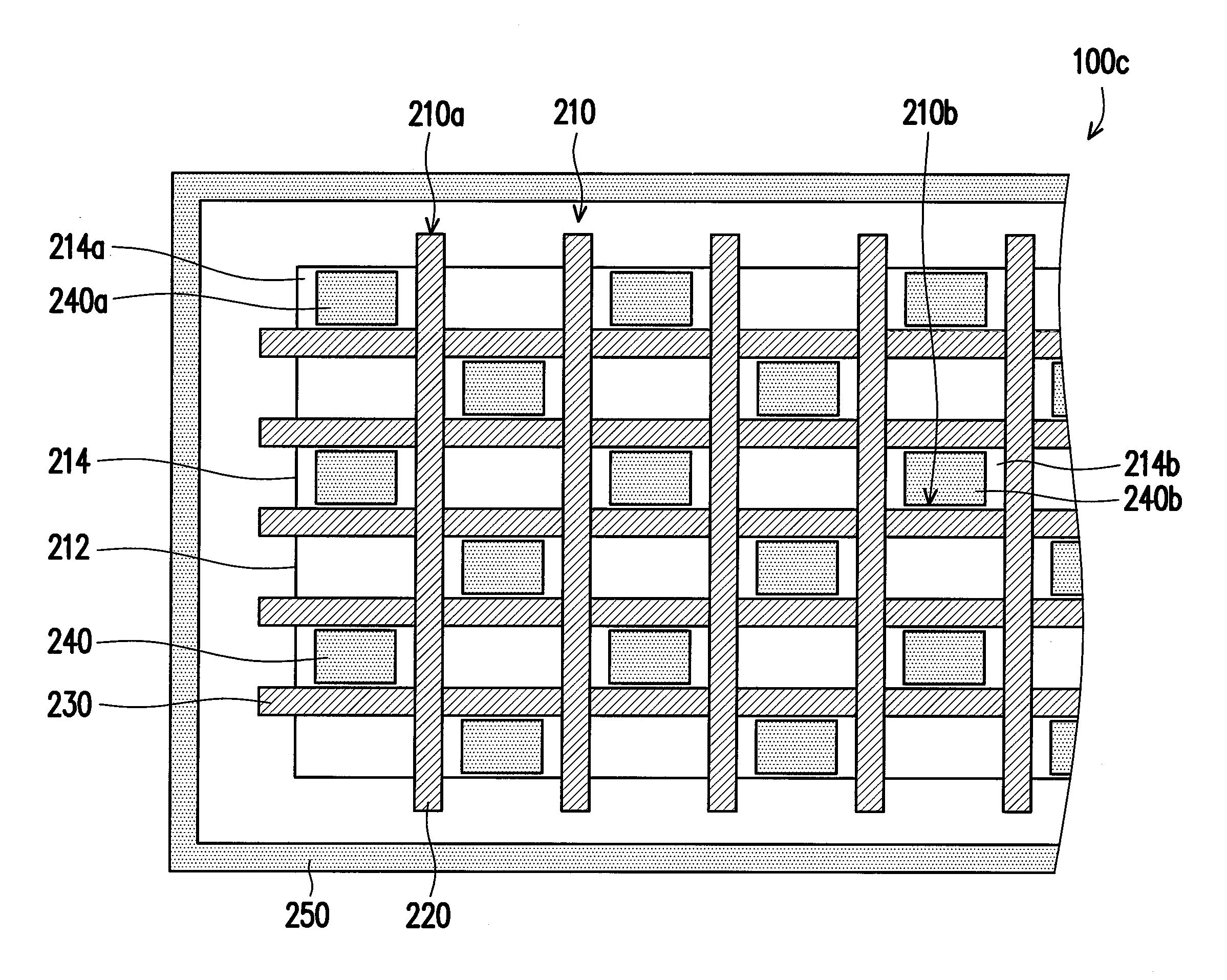
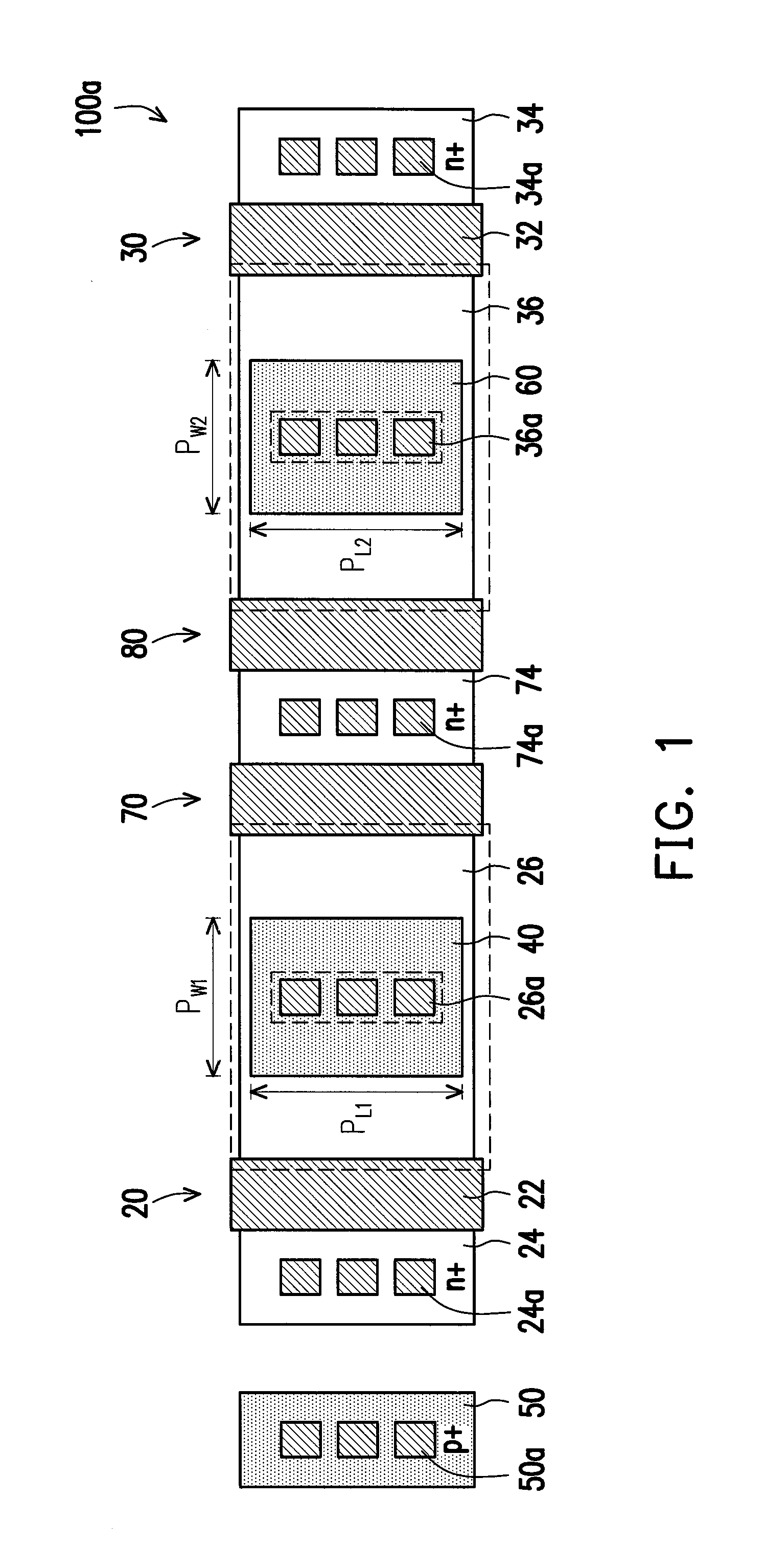
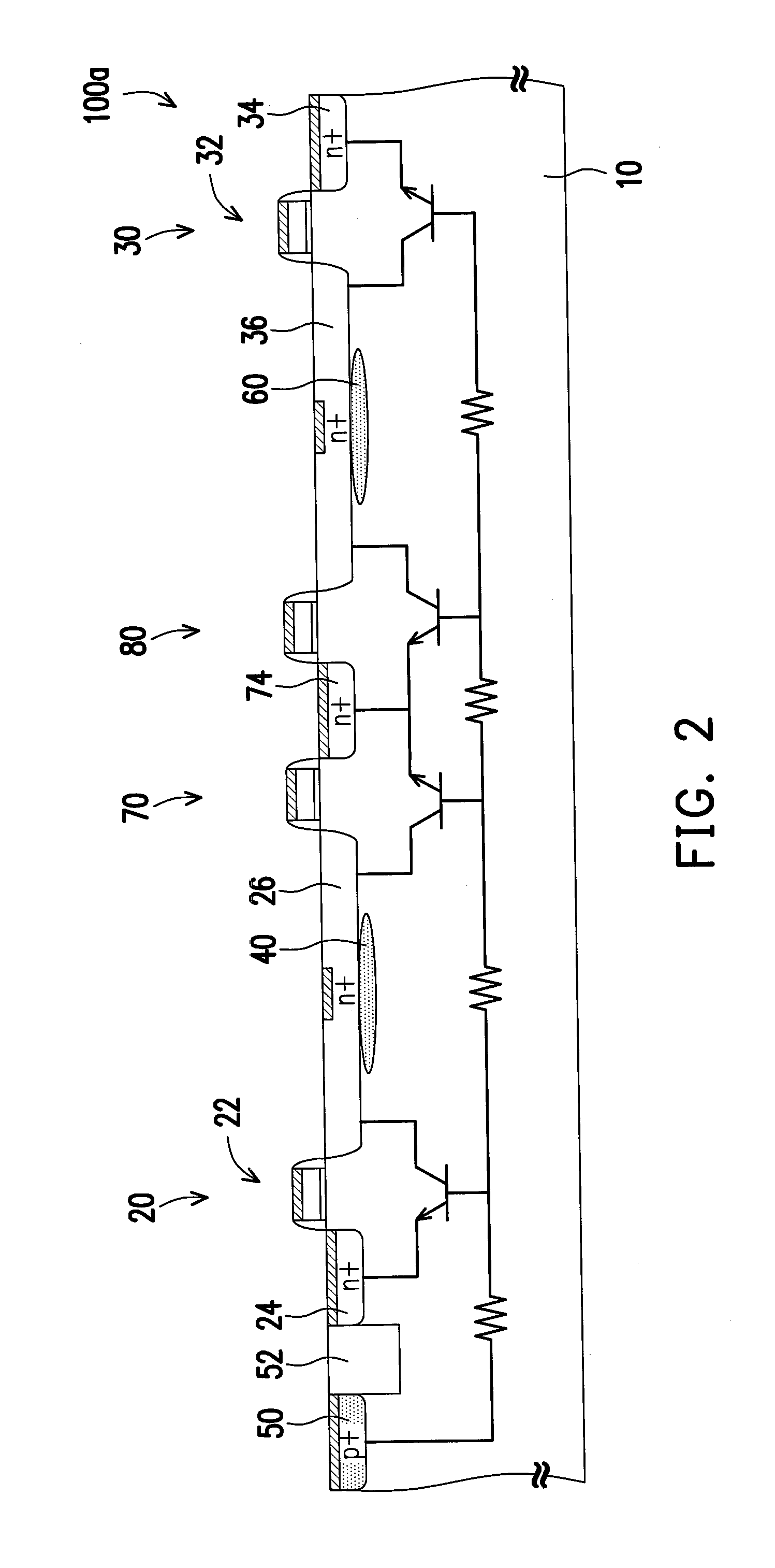
[0029]In an embodiment of the invention, the ESD protection structure includes a plurality of MOS devices, doped regions are respectively located under drain regions of the MOS devices, and the drain regions have a conductivity type different from that of the doped regions. The robustness of the ESD protection structure can be improved by such disposition. Besides, the doped region close to the pick-up region has a greater area / doping concentration than that of the doped region away from the pick-up region, so that the breakdown voltages of the parasitic bi-polar junction transistors can be substantially equal, and the respective bi-polar junction transistors can be turned on almost at the same time....


PUM


Abstract

Provided is an electrostatic discharge (ESD) protection structure including a substrate, a pick-up region, a first MOS device, a second MOS device, a first doped region and a second doped region. The pick-up region is located in the substrate. The first MOS device has a first drain region of a first conductivity type located in the substrate. The second MOS device has a second drain region of the first conductivity type located in the substrate. The first drain region is closer to the pick up region than the second drain region is. The first doped region of a second conductivity type is located under the first doped region. The second doped region of the second conductivity type is located under the second doped region. The area and / or doping concentration of the first doped region is greater than that of the second doped region.

Description

BACKGROUND OF THE INVENTION[0001]1. Field of Invention[0002]The present invention relates to a semiconductor device, and more particularly to an electrostatic discharge (ESD) protection structure.[0003]2. Description of Related Art[0004]ESD is a phenomenon in which charges are accumulated on a non-conductor or a non-grounded conductor and then suddenly transfer and discharge through a discharge path. The circuits in ICs can be damaged by ESD. For example, a charge carrying object, such as a human body, a machine for packaging ICs or an apparatus for testing ICs, can discharge to an IC chip when the charge carrying object is in contact with the IC chip. Thus, the IC chip is damaged or broken by the transient power of ESD.[0005]Usually the ESD tolerance for commercially available ICs is required to pass the human body mode (HBM) test at 2 kV and the machine model (MM) test at 200 V. In order to sustain the above-mentioned high-voltage ESD tests, the large-sized ESD protection device f...

Claims


Application Information

Patent Timeline
08 Jan 2015
Publication
US20150008529A1
IPC
H01L27/02; H01L27/06
CPC
H01L27/0623; H01L27/0248; H01L27/0277
Inventors
WEN, YUNG-JU; WANG, CHANG-TZU