
Monitoring and Controlling Temperatures in a Semiconductor Structure

a technology of semiconductor structure and monitoring temperature, applied in the field of components, can solve the problems of high temperature damage to the semiconductor device, overheating of the semiconductor, and large currents,

Active Publication Date: 2015-01-29
INFINEON TECH AG
View PDF8 Cites 4 Cited by
  • Summary
  • Abstract
  • Description
  • Claims
  • Application Information

AI Technical Summary

Benefits of technology

The patent describes semiconductor devices and methods to solve problems such as overheating and excessive noise in electronic devices. The technical effects of this invention include reducing the likelihood of device failure and improving overall performance.

Problems solved by technology

As is known a semiconductor device may be damaged by high temperatures, since for example the silicon will exhibit so-called thermal exhaustion symptoms, e.g., metallization of the silicon.
In operation there are some situations prone to cause overheating of a semiconductor, particularly when large currents flow through the semiconductor.
Furthermore, large currents may occur in case of a short-cut at the load.
As a consequence the semiconductor may be further heated, which may cause damages of the semiconductor structure.

Method used


Image

  • Monitoring and Controlling Temperatures in a Semiconductor Structure
  • Monitoring and Controlling Temperatures in a Semiconductor Structure
  • Monitoring and Controlling Temperatures in a Semiconductor Structure

Examples


Embodiment Construction

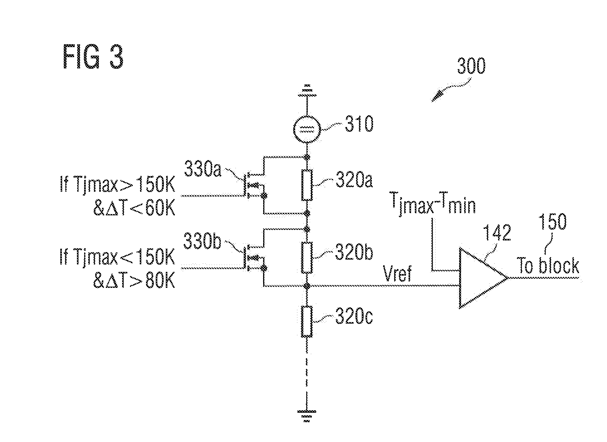
[0013]FIG. 1 depicts a block diagram of an electronic semiconductor device 100 comprising a semiconductor structure 110 and at least a first means for determining the highest temperature of the device and another means for determining the lowest temperature of the device. Note that the temperature determining devices shall be located at the probably hottest spot and the probably coldest spot on the device. Typically, the hottest spot of the semiconductor device 100 is around the area exhibiting the highest power density, whereas the lowest spot may at a location exhibiting a small or negligible power density. Accordingly, the hottest spot may be located close to a bond wire serving as a power supply of the device. In the depicted embodiment the temperature determining devices are exemplified by element 120 and element 130, since the exemplifying circuit comprises only this semiconductor structure for demonstration purposes. Note that these locations shall not limit the placing of th...


PUM


Abstract

An electronic device includes a semiconductor structure. A first temperature sensor is located at a hot spot of the semiconductor structure and a second temperature sensor is located at a cold spot of the semiconductor structure. A control block is configured to control current flow through the semiconductor structure. For example, the control block is configured to cut off the current flow through the semiconductor structure when a temperature at the hot spot exceeds a first predefined threshold or when a temperature difference between the temperature at the hot spot and a temperature at the cold spot exceeds a second predefined threshold.

Description

TECHNICAL FIELD[0001]The present invention relates generally to components and, in particular embodiments, to monitoring and controlling temperatures in semiconductor structures.BACKGROUND[0002]Semiconductor devices generally generate heat whenever a high power is applied to the semiconductor since each semiconductor device exhibits an ohmic resistance that burns some electrical power into heat. As is known a semiconductor device may be damaged by high temperatures, since for example the silicon will exhibit so-called thermal exhaustion symptoms, e.g., metallization of the silicon. Accordingly, the temperature of a semiconductor structure should not exceed a predefined limit to prevent such damage.[0003]To limit the temperature of a semiconductor structure the current flow through the structure can be shut down in case a predefined temperature limit is exceeded. In conventional chips or integrated circuits the temperature is measured at the estimated hottest and at the estimated col...

Claims


Application Information

Patent Timeline
Patent Type & Authority Applications(United States)
IPC IPC(8): H01L23/34
CPCH01L23/34H01L27/0255H01L2924/0002H01L2924/00
Inventor KARTAL, VELI
Owner INFINEON TECH AG
Learn More