Package structure of an optical module

Inactive Publication Date: 2015-01-29
LINGSEN PRECISION INDS
View PDF18 Cites 11 Cited by
  • Summary
  • Abstract
  • Description
  • Claims
  • Application Information

AI Technical Summary

Benefits of technology

[0006]The main objective of the present invention is to provide a package structure of an optical module to effectively impro

Problems solved by technology

However, after the proximity of the conventional optical sensing module in the package is complete, the power of the light emitted by the light emitting chip of the module often has been greatly reduced after the light is reflecte

Method used


Image

  • Package structure of an optical module
  • Package structure of an optical module
  • Package structure of an optical module

Examples


Embodiment Construction

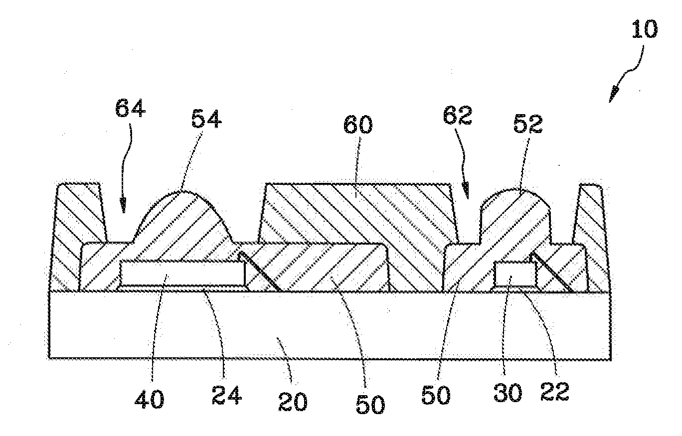
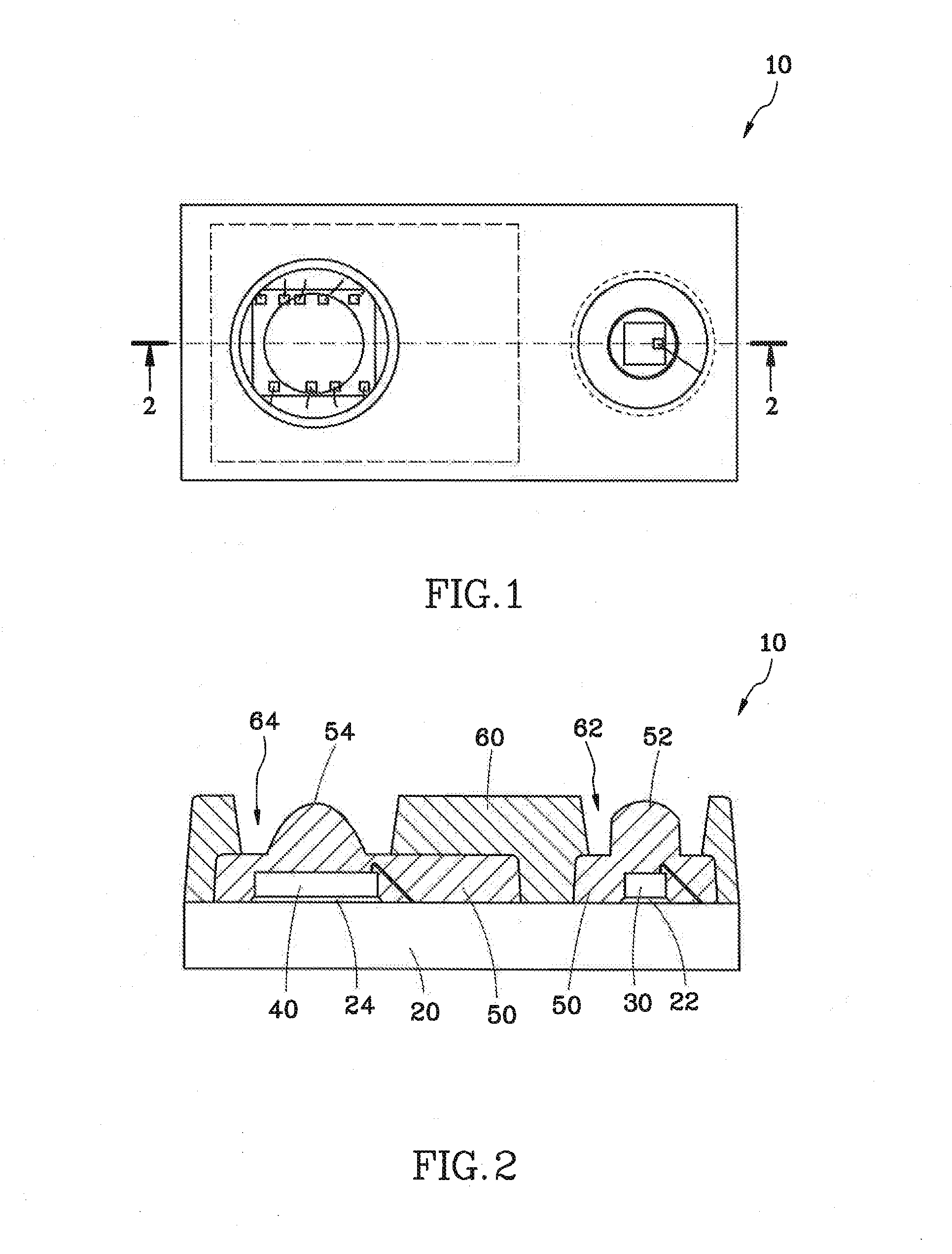
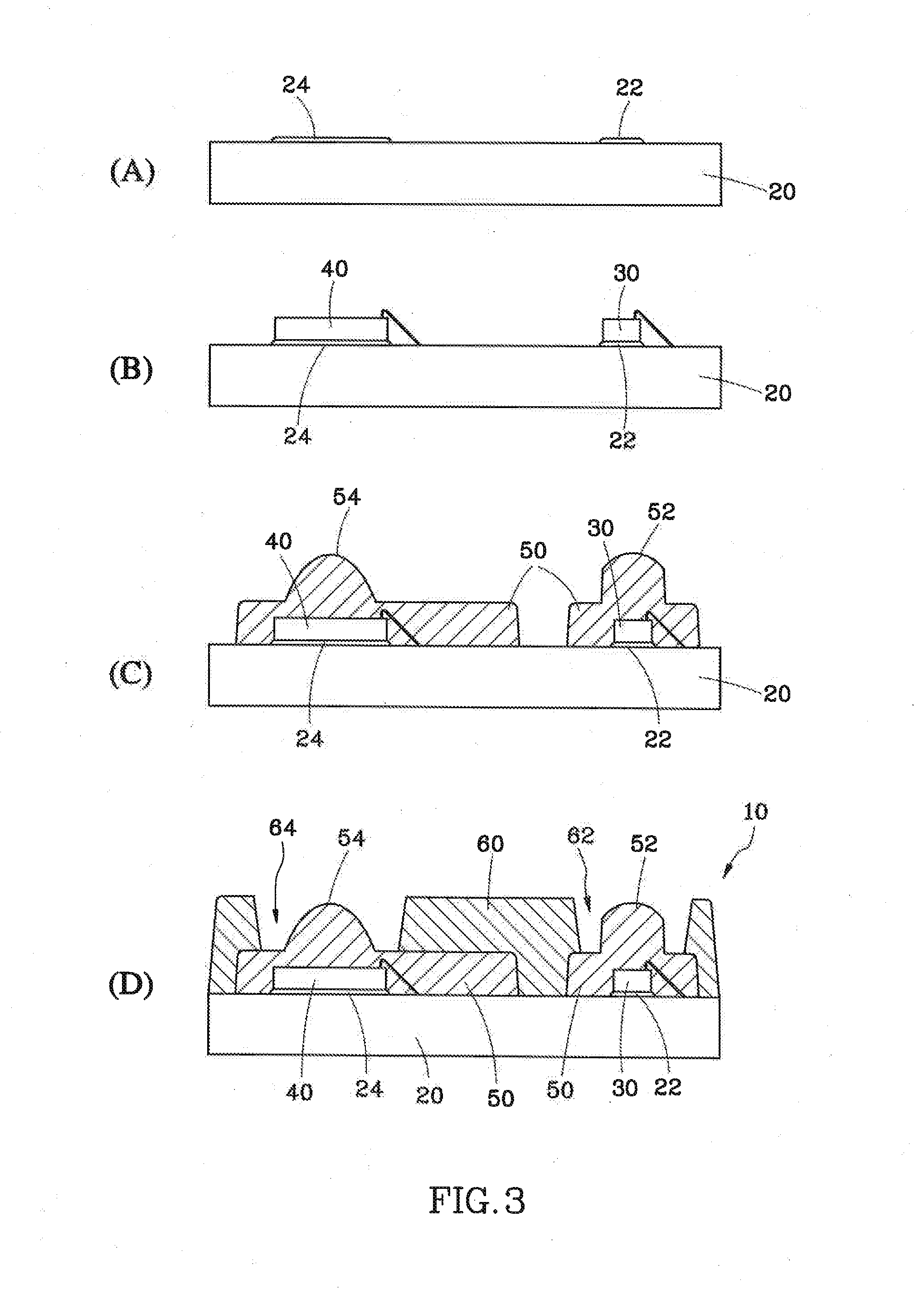
[0028]Please refer to FIG. 1 and FIG. 2. The package structure of an optical module 10 provided by a preferred embodiment of the present invention is cut from a module of the package array and comprises a substrate 20, a light receiving chip 30, a light emitting Chip 40, two encapsulating gels 50 and a cover 60.

[0029]The substrate 20 in the preferred embodiment is a non-ceramic substrate, such as a Bismaleimide Triazine (known as BT) substrate or a glass fiber (known as FR4) substrate made of organic materials. Thereby, the material cost of the substrate 20 is low. The surface of the substrate 20 is defined with a light receiving region 22 and a light emitting region 24.

[0030]The light emitting chip 30 and the light receiving chip 40 are treated by a die attaching process and a wire bonding process and are disposed on the light receiving region 22 and the light emitting region 24 of the substrate 20. The light emitting chip 30 is used to emit light, and the light receiving chip 40 i...


PUM


Abstract

The present invention relates to a package structure of an optical module. The light emitting chip and the light receiving chip are disposed on the light emitting region and the light receiving region of the substrate, respectively. Two encapsulating gels are coated on the light emitting chip and the light receiving chip to form a first and a second hemispherical lens portions thereon, respectively. A cover is affixed on the substrate and each of the encapsulating gels and has a light emitting hole and a light receiving hole, where the first and second lens portions are accommodated, respectively. In this way, the package structure of an optical module of the present invention can be made with the encapsulating gels of different curvatures according to different needs to improve the luminous efficiency of the light emitting chip effectively and to improve the reception efficiency of the light receiving chip.

Description

BACKGROUND OF THE INVENTION[0001]1. Field of the Invention[0002]The present invention relates to a package structure, especially related to a package structure of an optical module.[0003]2. Descriptions of the Related Art[0004]Currently, optical proximity sensing modules have become a mainstream technology choice of the new generation of intelligent electronic devices (such as smart phones). When the electronic device is close to someone's ears (face detection) or placed in a pocket, the module will immediately turn off the screen display to save power and prevent accidental screen presses to provide a better user experience. The action principle of the module is emitting a light source with a light emitting chip, such as a light emitting diode (LED), the light is reflected by the surface of an object and is then projected onto a light receiving chip to be converted to electrical signals for subsequent processing.[0005]However, after the proximity of the conventional optical sensing...

Claims


Application Information

Patent Timeline
IPC IPC(8): H01L33/52H01L31/173
CPCH01L31/173H01L33/52H01L25/167H01L2224/32225H01L2224/48091H01L2224/48227H01L2224/73265H01L2224/83192G01S7/4813H01L31/02325G01S17/04H01L2924/00014H01L2924/00
Inventor TU, MING-TECHEN, YU-SHIANG
Owner LINGSEN PRECISION INDS
Why Eureka
Try Eureka