Organic el display device

Active Publication Date: 2015-02-26
JAPAN DISPLAY INC
View PDF9 Cites 27 Cited by
  • Summary
  • Abstract
  • Description
  • Claims
  • Application Information

AI Technical Summary

Benefits of technology

[0016]Also, in the organic EL display device according to the present invention, each of the contact holes may further include control signal lines that extend along between

Problems solved by technology

However, the contact hole has a large step, and the light emitting element cannot be normally formed.
JP 2009-301058 A discloses an example in which the light emitting area is enlarged,

Method used


Image

  • Organic el display device
  • Organic el display device
  • Organic el display device

Examples


Example

First Embodiment

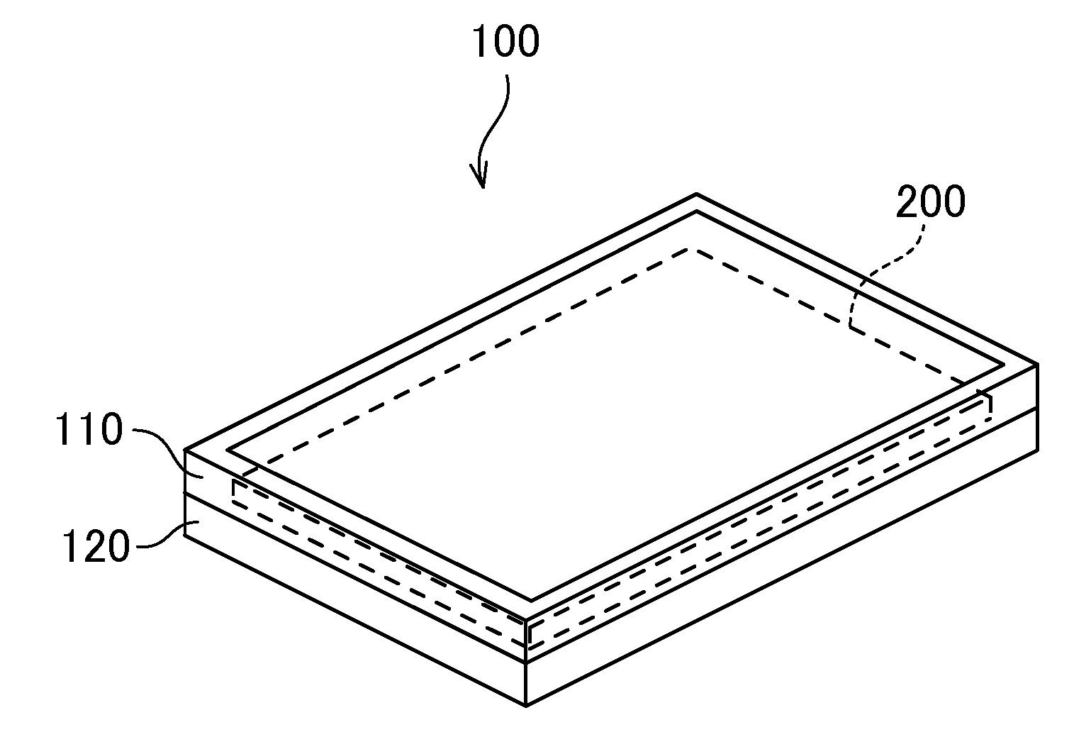
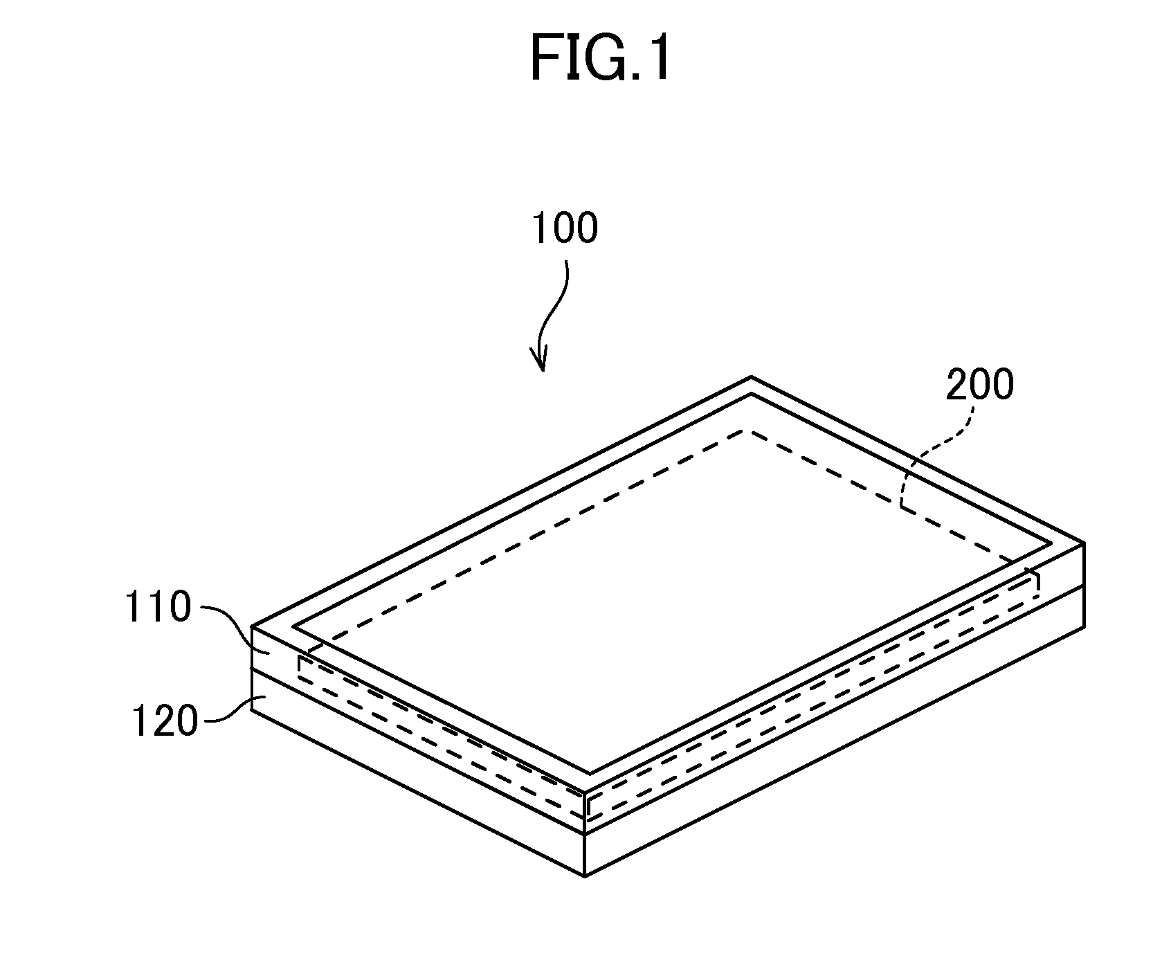
[0036]FIG. 1 is a diagram schematically illustrating an organic EL display device 100 according to a first embodiment of the present invention. As illustrated in FIG. 1, the organic EL display device 100 includes an organic EL panel 200 fixedly held between an upper frame 110 and a lower frame 120.

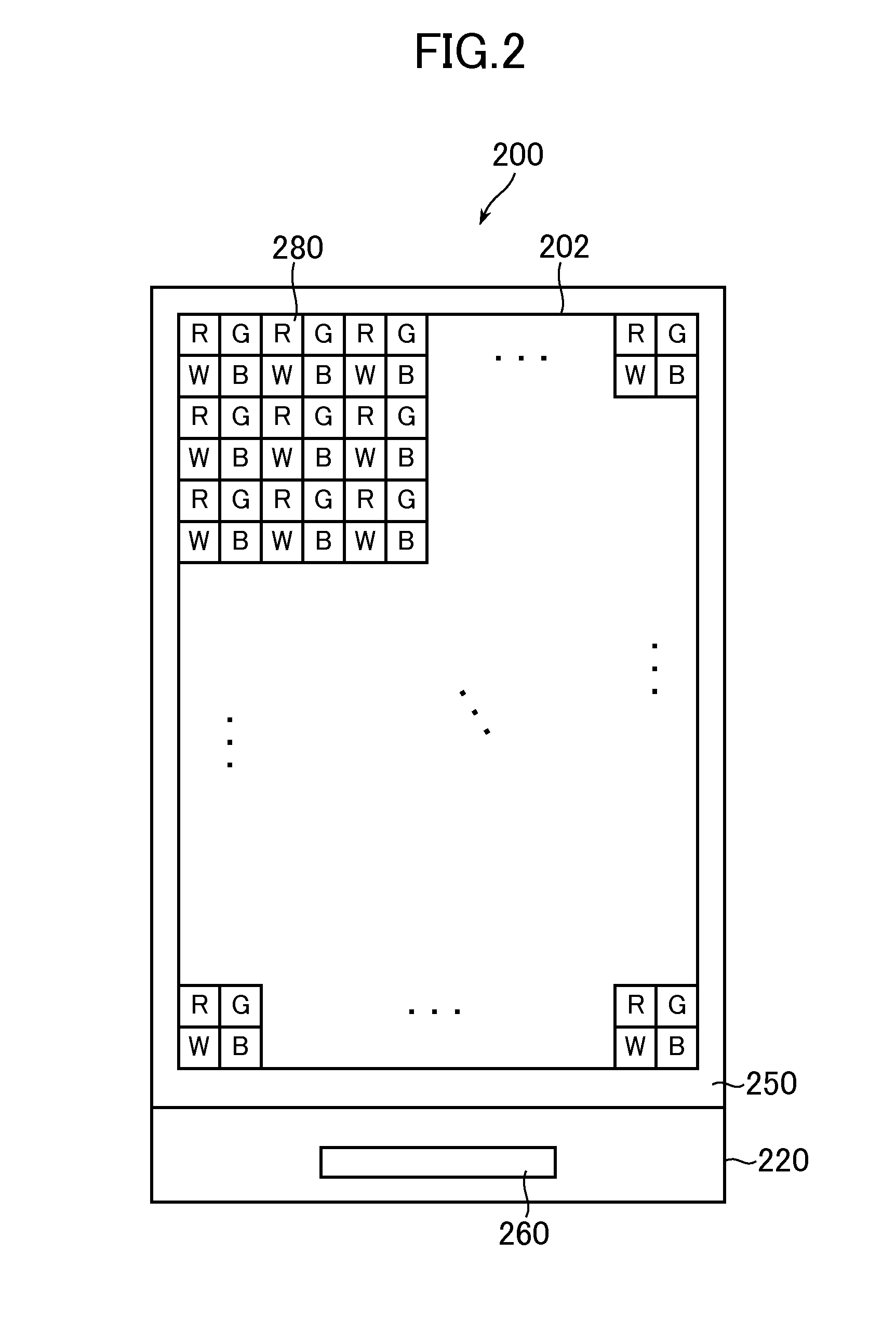
[0037]FIG. 2 is a diagram illustrating a configuration of the organic EL panel 200 in FIG. 1. The organic EL panel 200 includes two substrates of a TFT (thin film transistor) substrate 220 and a sealing substrate 250, and a space between those substrates 220 and 250 is filled with a transparent resin 241 (refer to FIG. 5). The TFT substrate 220 includes sub-pixels 280 which are arranged in a matrix in a display area 202. Also, a drive IC (integrated circuit) 260 which is a driver circuit that applies a potential for conducting between a source and a drain of a pixel transistor is applied to a scanning signal line (not shown) of the pixel transistor arranged in each of the s...

Example

Second Embodiment

[0050]Subsequently, an organic EL display device according to a second embodiment of the present invention will be described. The overall configurations of the organic EL display device and an organic EL panel according to the second embodiment are identical with those of the organic EL display device 100 and the organic EL panel 200 according to the first embodiment illustrated in FIGS. 1 to 3, and therefore a repetitive description will be omitted.

[0051]FIG. 12 is a diagram illustrating the four sub-pixels 280 configuring the pixel of FIG. 3 according to the second embodiment, which illustrates contact holes 381 according to this embodiment. As illustrated in FIG. 12, the light emitting area 282 of each sub-pixel 280 is surrounded by a scanning line 311, a first control line 312, and a second control line 313 which extend in a horizontal direction, and a signal line 314 and a power line 315 which extend in a vertical direction. The contact holes 381 are coupled wi...


PUM


Abstract

An organic EL display device includes: thin film transistors that are arranged in respective pixels within a display area which are arranged in a matrix; a planarization film that is formed over the thin film transistor and made of an organic insulating material; contact electrodes that are connected to drains or sources of the respective thin film transistors through contact holes formed within the planarization film; contact hole planarization films that are arranged over the respective contact electrodes with which the contact holes are embedded, and made of an organic insulating material; a lower electrode that is formed to be electrically connected onto the contact electrodes, and formed over the contact hole planarization film; and an organic layer that is arranged over the lower electrode to cover the overall display area, and formed of a plurality of organic material layers including a light emitting layer.

Description

CROSS-REFERENCE TO RELATED APPLICATION[0001]The present application claims priority from Japanese application JP2013-171765 filed on Aug. 21, 2013, the content of which is hereby incorporated by reference into this application.BACKGROUND OF THE INVENTION[0002]1. Field of the Invention[0003]The present invention relates to an organic EL display device.[0004]2. Description of the Related Art[0005]In recent years, an image display device (hereinafter referred to as “organic EL (electro luminescent) display device”) using self-luminous bodies called “organic light emitting diodes” has been input into practical use. As compared with a conventional liquid crystal display device, the organic EL display device not only is excellent in visibility and response speed, but also requires no auxiliary lighting device such as a backlight because of the use of the self-luminous bodies. Therefore, the organic EL display device can be further thinned.[0006]As a method of conducting color display in t...

Claims


Application Information

Patent Timeline
IPC IPC(8): H01L27/32
CPCH01L27/3248H10K59/351H10K59/123H10K59/124
Inventor FURUIE, MASAMITSUSATO, TOSHIHIROMIYAMOTO, MITSUHIDE
Owner JAPAN DISPLAY INC
Why Eureka
Try Eureka