

Snubber circuit and buffering method for snubber circuit
a snubber circuit and circuit technology, applied in the field of snubber circuits, can solve the problems of power loss and decrease the power conversion efficiency of switching power supplies, and achieve the effect of reducing/eliminating power losses and long reverse recovery tim
- Summary
- Abstract
- Description
- Claims
- Application Information
AI Technical Summary
Benefits of technology
Problems solved by technology
Method used
Image

Examples
Embodiment Construction
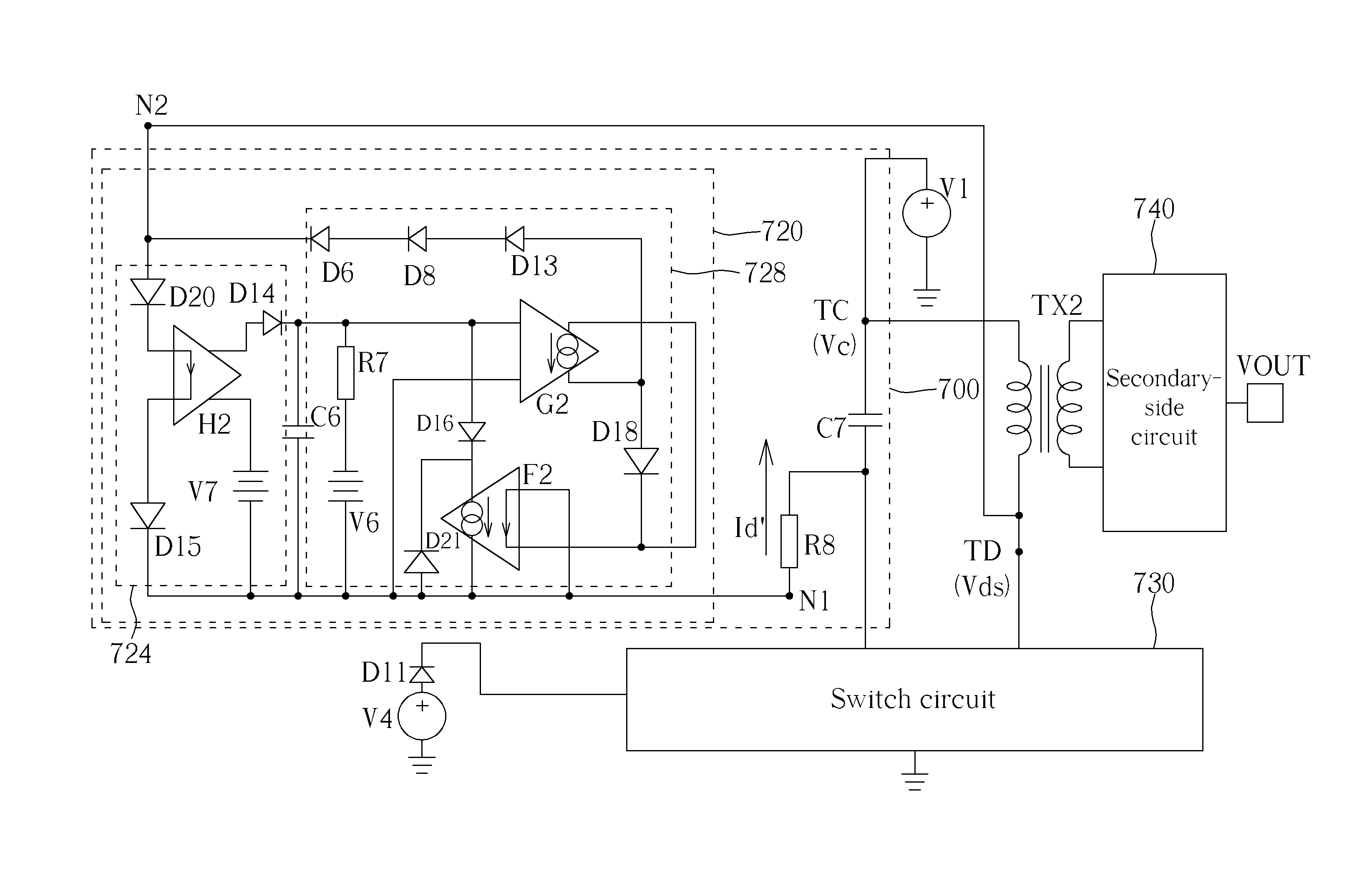
[0030]In order to realize a snubber circuit capable of being employed in high speed switching applications and having low power consumption, a conventional snubber is tested and analyzed to obtain circuit characteristics thereof. Next, a buffer device employed in a snubber circuit is proposed according to test / analysis results. Further description is detailed below.
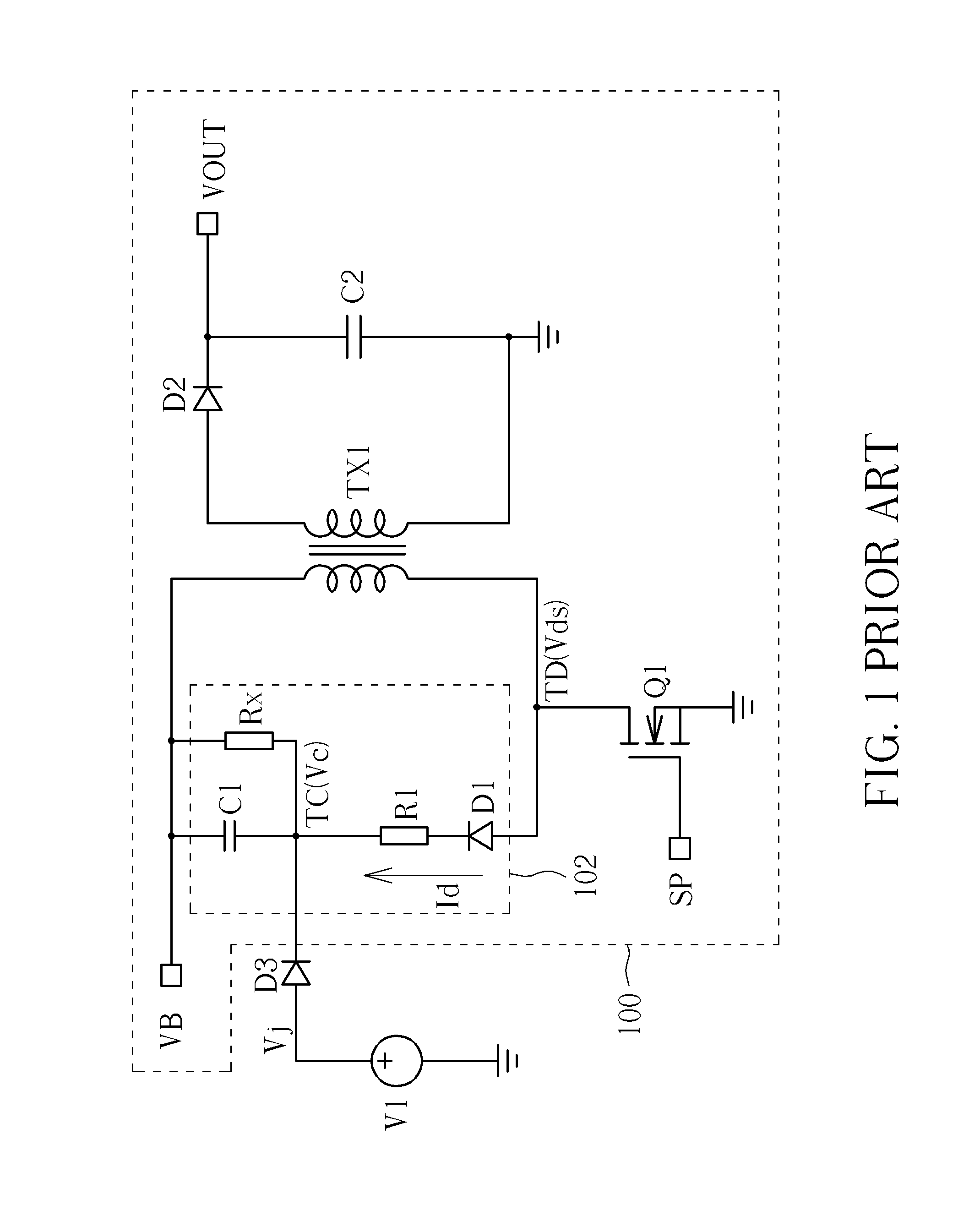
[0031]Please refer to FIG. 1 again. FIG. 1 further illustrates a circuit architecture for testing a conventional snubber according to an embodiment of the present invention. As shown in FIG. 1, the RCD snubber 102 is disposed on a primary side of the DC-to-DC converter 100 including the transformer TX1, the switch Q1, a diode D2 and a capacitor C2. As a person skilled in the art should understand that the DC-to-DC converter 100 converts an input voltage VB into an output voltage VOUT according to a control signal SP (e.g. a pulse width modulation (PWM) signal), further description is omitted here for brevity. The circuit ...
PUM
 Abstract
Description
Claims
Application Information