Method for separation between an active zone of a substrate and its back face or a portion of its back face
- Summary
- Abstract
- Description
- Claims
- Application Information
AI Technical Summary
Problems solved by technology
Method used
Image

Examples
Example
[0083]Identical, similar or equivalent parts of the different figures have the same numeric references to facilitate comparisons between the different figures.
[0084]The different parts shown in the figures are not necessarily at the same scale, to make the figures more easily readable.
DETAILED PRESENTATION OF PARTICULAR EMBODIMENTS
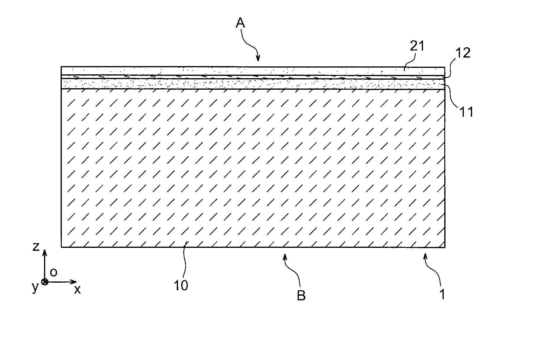
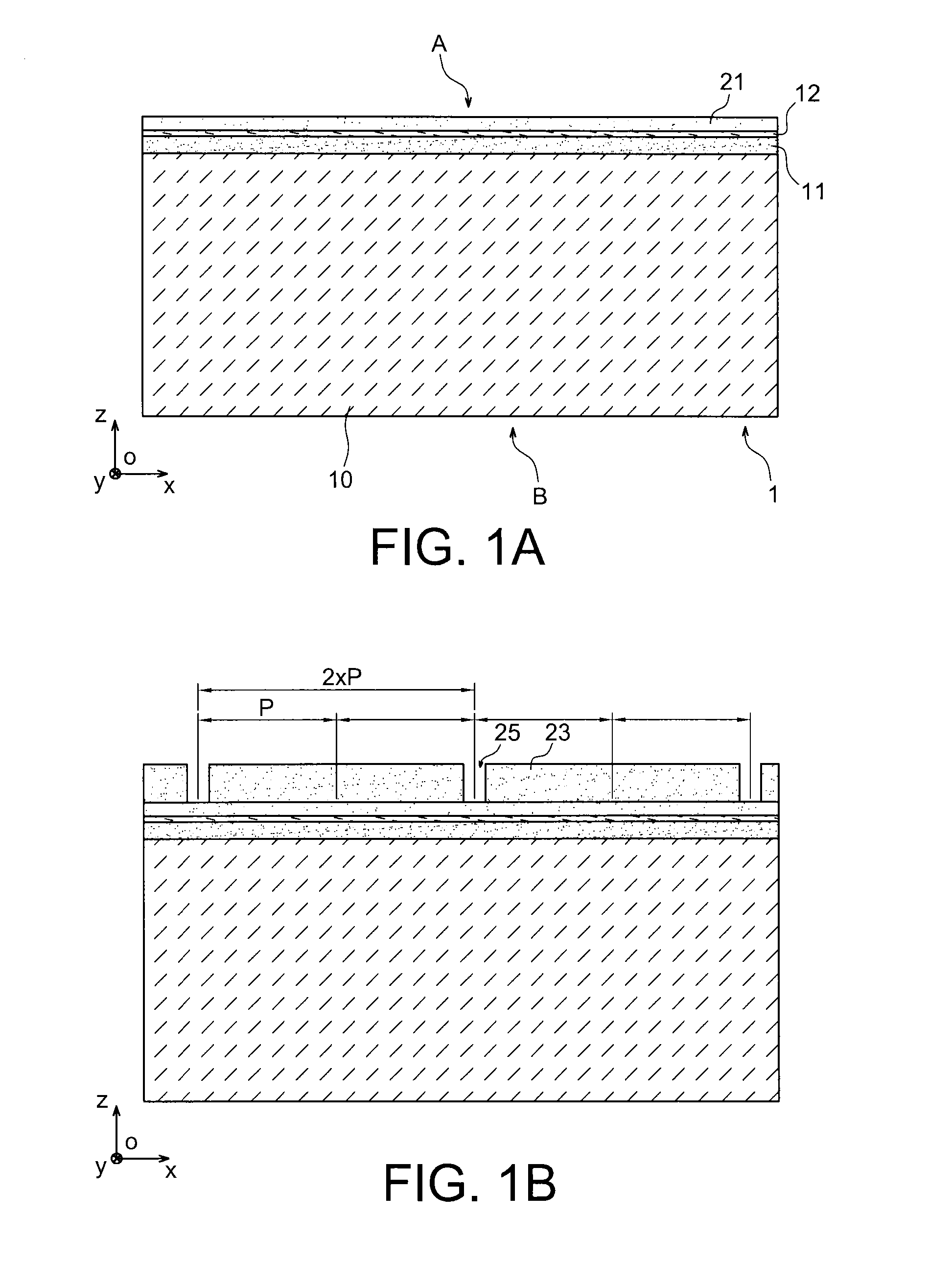
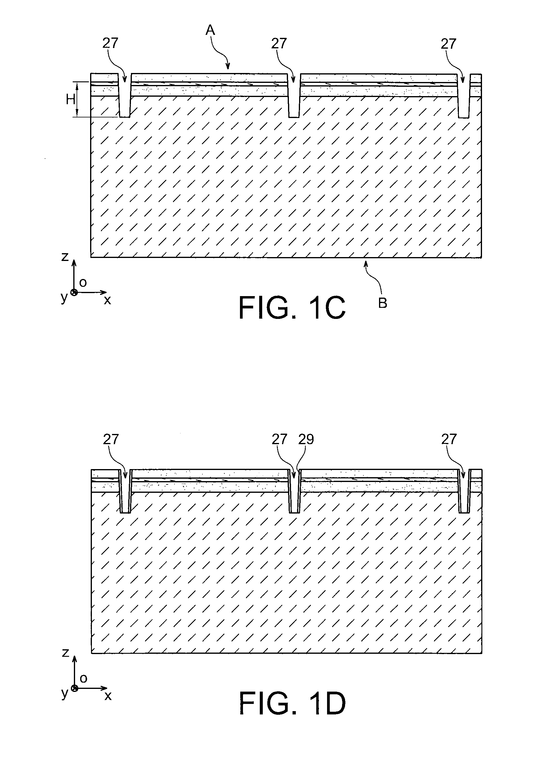
[0085]A first example method according an embodiment of the invention will now be described with reference to FIGS. 1A-1K.
[0086]The initial material for this method may for example be a semiconductor on insulator (SOI) type substrate.
[0087]The substrate 1 thus comprises a support layer, for example a semiconducting layer 10 that may be based on Si, for example between 400 μm and 1 mm thick (measured along a direction parallel to the z axis of a orthogonal coordinate system [O;x;y;z] given in FIG. 1A).
[0088]The substrate 1 may also include an insulating layer 11, for example based on silicon oxide, located on and in contact with the support layer 10. The in...
PUM
 Abstract
Description
Claims
Application Information
 - R&D Engineer
- R&D Manager
- IP Professional
- Industry Leading Data Capabilities
- Powerful AI technology
- Patent DNA Extraction
Browse by: Latest US Patents, China's latest patents, Technical Efficacy Thesaurus, Application Domain, Technology Topic.
© 2024 PatSnap. All rights reserved.Legal|Privacy policy|Modern Slavery Act Transparency Statement|Sitemap