Semiconductor thin film forming method, production methods for semiconductor device and electrooptical device, devices used for these methods, and semiconductor device and electrooptical device

a technology of semiconductor devices and thin films, applied in the direction of drying, lighting and heating apparatus, furnaces, etc., can solve the problems of increasing the cost of apparatus, poor productivity, and difficulty in obtaining crystals with a grain size of 500 nm or mor

Inactive Publication Date: 2007-02-27
SONY CORP
View PDF38 Cites 401 Cited by
  • Summary
  • Abstract
  • Description
  • Claims
  • Application Information

AI Technical Summary

Benefits of technology

[0011]In forming a polycrystalline or a single crystalline semiconductor thin-film on a substrate, or in forming a semiconductor device having a polycrystalline or a single crystalline semiconductor thin-film on a substrate, a method for forming a semiconductor thin-film or for manufacturing a semiconductor device, according to the present invention, comprises a first step of forming a low-crystallization semiconductor thin-film on the substrate, and a second step of heating and cooling the low-crystallization semiconductor thin-film to a fusion, a semi-fusion, or a non-fusion state by flash lamp annealing to facilitate the crystallization of the low-crystallization semiconductor thin-film.

Problems solved by technology

As a result, even when a method is performed in which substrate temperature is heated to approximately 400° C. while short wavelength and short pulse laser is emitted, and in which hydrogen, oxygen, and the like which inhibit the crystal growth are sufficiently removed so as to control the solidification speed, it has been difficult to obtain crystals having a grain size of 500 nm or more.
However, there have been a number of problems, such as unstable excimer laser output, poor productivity, increase in cost of apparatus due to increased size thereof, lower yield, degradation in quality, and the like, and in particular, when a large glass substrate having a size of 1 meter by 1 meter is used, the problems mentioned above become more serious, and as a result, it becomes more difficult to improve performance and quality and to reduce cost.
However, the process is complicated, sufficient gettering effect cannot be obtained, semiconductor properties of the silicon film are degraded, and the stability and the reliability of elements thus formed are degraded.
Hence, it is difficult to reduce cost, and the applications are limited to EVF and data / AV projectors.
In a catalytic CVD method, without performing anneal for crystallization, a carrier mobility of approximately 30 cm2 / V·sec has been obtained; however, the value mentioned above is not large enough to manufacture superior MOSTFTs.
In addition, when a polycrystalline silicon film is formed on a glass substrate, amorphous silicon in an initial transition state (a thickness of 5 to 10 nm) may be easily formed depending on film-forming conditions, and when a bottom-gate MOSTFT is formed, it is difficult to obtain desired carrier mobility.
In general, in an LCD which uses polycrystalline silicon MOSTFTs and which is integrated with driving circuits, bottom-gate MOSTFTs are preferably formed in view of yield and productivity; however, the problem described above has been still serious.

Method used


Image

  • Semiconductor thin film forming method, production methods for semiconductor device and electrooptical device, devices used for these methods, and semiconductor device and electrooptical device
  • Semiconductor thin film forming method, production methods for semiconductor device and electrooptical device, devices used for these methods, and semiconductor device and electrooptical device
  • Semiconductor thin film forming method, production methods for semiconductor device and electrooptical device, devices used for these methods, and semiconductor device and electrooptical device

Examples


first embodiment

[0217

[0218]Referring to FIGS. 1 to 33, a first embodiment of the present invention will be described.

[0219]In this embodiment, the present invention is applied to a top gate type polycrystalline silicon CMOS (Complementary MOS) TFT.

[0220]

[0221]A catalytic CVD method used for this embodiment will first be described. In the catalytic CVD method, reacting gases composed of a hydrogen-based carrier gas and a source gas such as a silane gas are brought into contact with a heated catalyst such as tungsten so as to impart high energy to radicals depositing species, precursors thereof, hydrogen-based active species such as activated hydrogen ions, and subsequently, a low-crystallization semiconductor thin-film such as microcrystalline silicon containing amorphous silicon is deposited on a substrate by vapor-phase growth.

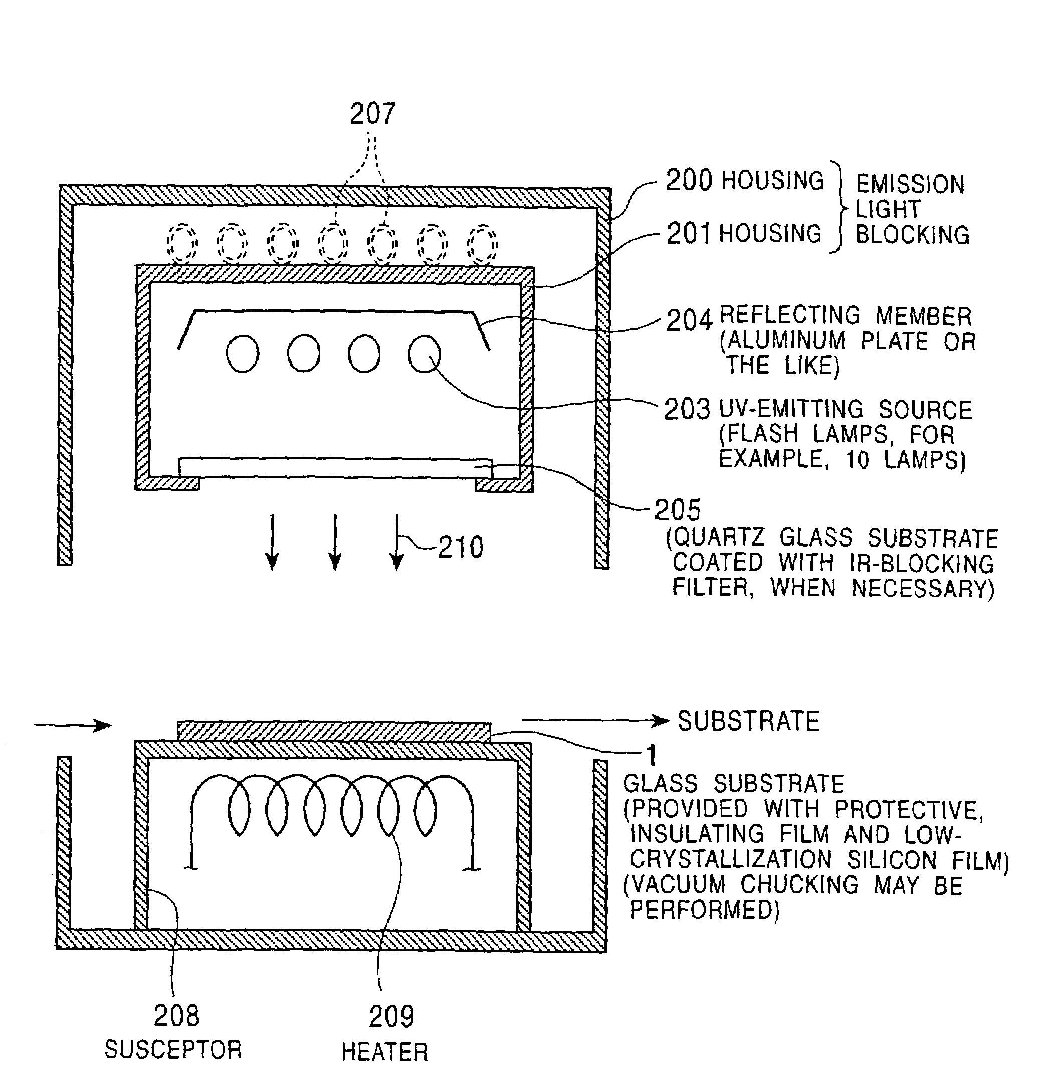
[0222]This catalytic CVD may be performed by using an apparatus as shown in FIGS. 5 and 6.

[0223]According to this apparatus, a gas composed of a hydrogen-based carrier gas a...

second embodiment

[0464

[0465]

[0466]In this embodiment, the present invention is applied to an LCD (liquid crystal display device) using a polycrystalline silicon MOSTFT formed by a high temperature process, and hereinafter, a manufacturing example therefor will be described.

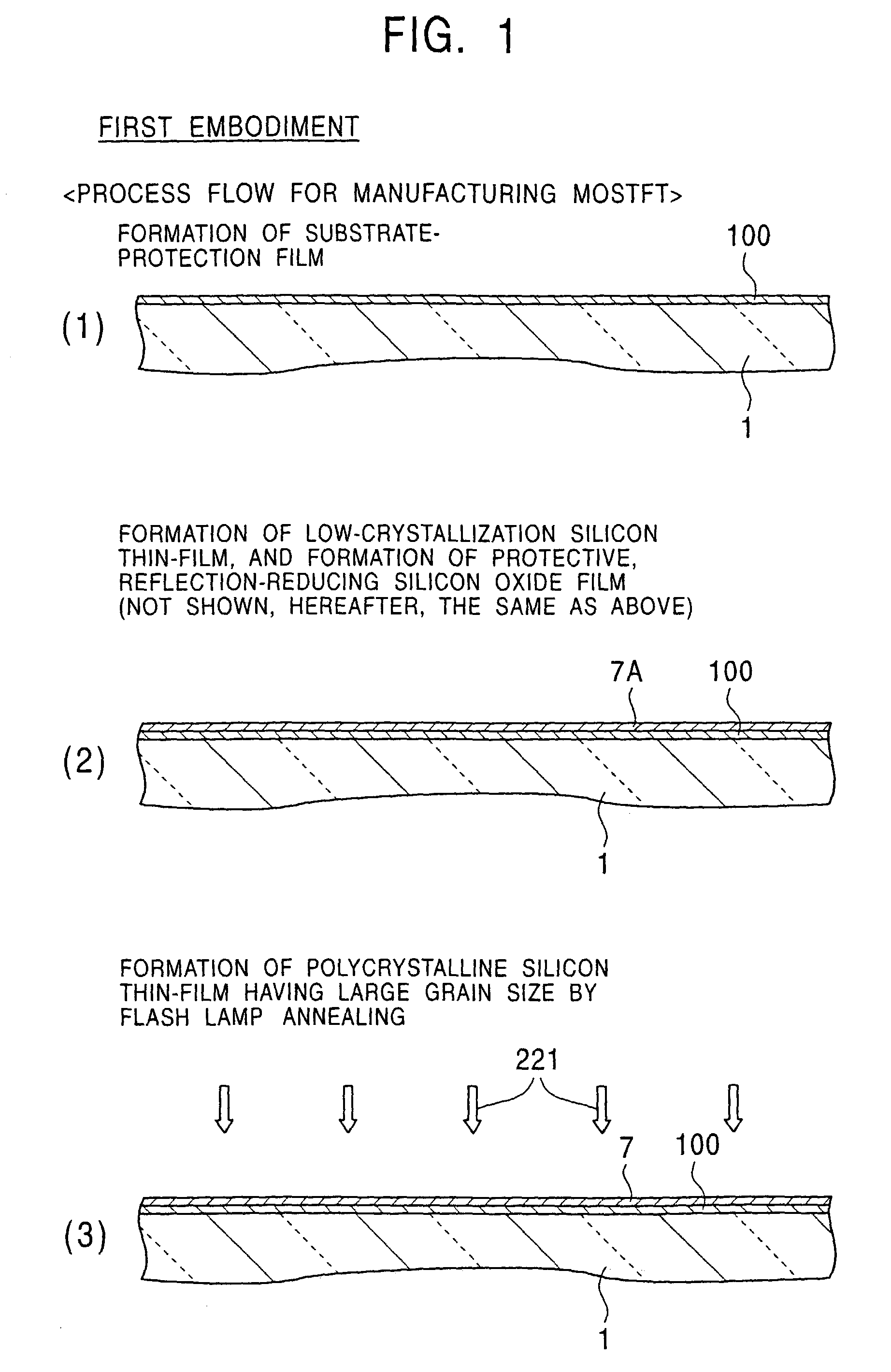
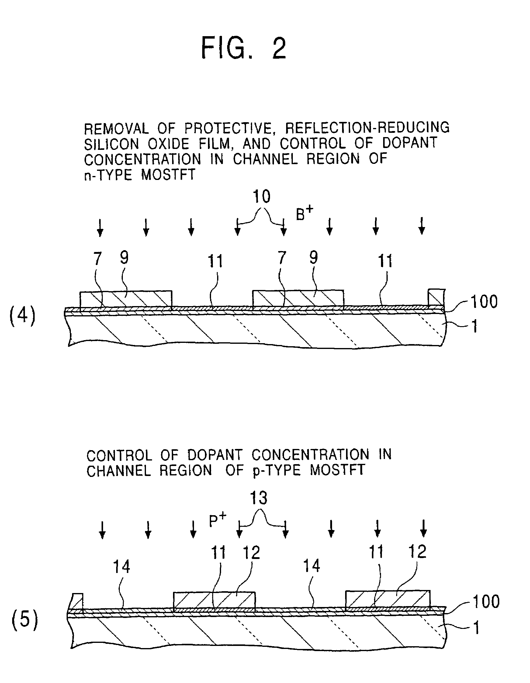
[0467]First, as shown in FIG. 34(1), in a pixel portion and a peripheral circuit portion, a substrate-protection film 100 (not shown in the figure, and hereafter, the same as described above) is formed on one major surface of a heat resistant substrate 61 (a strain point of approximately 800 to 1,100° C., and a thickness of 50 μm to several millimeters) composed of quartz glass or crystallized glass by the catalytic CVD or the like described above, and on this protection film, a low-crystallization silicon thin-film 67A is formed by the catalytic CVD or the like described above. In addition, when necessary, a protective, reflection-reducing silicon oxide film (10 to 30 nm thick) is formed (not shown in this figure).

[0468]Next, as ...

third embodiment

[0554

[0555]In this embodiment, the present invention is applied to an organic or an inorganic electroluminescent (EL) display devices, such as an organic EL display device. Hereinafter, the structural examples and the manufacturing examples will be described. In this embodiment, a top gate type MOSTFT will be described, and it is naturally understood that the present invention be applied to a bottom gate type or a dual gate type MOSTFT.

[0556]

[0557]As shown in FIGS. 46(A) and (B), according to this structural example I, by using a polycrystalline silicon thin-film (or a single crystalline silicon thin-film: hereinafter, the polycrystalline silicon thin-film will be described by way of example; however, the same description thereof can also be applied to the single crystalline silicon thin-film), which may or may not contain tin and which has a large grain size and high crystallinity, formed on a substrate 111 composed of glass or the like by the method described above according to th...


PUM

PropertyMeasurementUnit
carrier mobilityaaaaaaaaaa
electron mobilityaaaaaaaaaa
grain sizeaaaaaaaaaa

Abstract

An object of the present invention is to provide a method for easily forming a polycrystalline semiconductor thin-film, such as polycrystalline silicon having high crystallinity and high quality, or a single crystalline semiconductor thin-film at inexpensive cost, the crystalline semiconductor thin-film having a large area, and to provide an apparatus for processing the method described above. In forming a polycrystalline (or single crystalline) semiconductor thin-film (7), such as a polycrystalline silicon thin-film, having high crystallinity and a large grain size on a substrate (1), or in forming a semiconductor device having the polycrystalline (or single crystalline) semiconductor thin-film (7) on the substrate (1), a method comprises forming a low-crystallization semiconductor thin-film (7A) on the substrate (1), and subsequently heating and cooling this low-crystallization semiconductor thin-film (7A) to a fusion, a semi-fusion, or a non-fusion state by flash lamp annealing to facilitate the crystallization of the low-crystallization semiconductor thin-film, whereby a polycrystalline (single crystalline) semiconductor thin-film (7) is obtained. A method for forming the semiconductor device and an apparatus for processing the methods are also disclosed.

Description

BACKGROUND OF THE INVENTION [0001]The present invention relates to methods and apparatuses for growing polycrystalline or a single crystalline semiconductor thin-film, such as polycrystalline silicon, single crystalline silicon, or the like, on a substrate, to methods and apparatuses for manufacturing semiconductor devices and electrooptic devices having the polycrystalline or the single crystalline semiconductor thin-film on the substrate, and to the semiconductor devices and the electrooptic devices.BACKGROUND ART[0002]Heretofore, when a source, a drain, and a channel region of a MOSFET (Metal-Oxide-Semiconductor Field Effect Transistor),such as a MOSTFT (Thin Film Transistor=thin-film insulating gate type field effect transistor) are formed, vapor-phase growth, such as plasma CVD (CVD: Chemical Vapor Deposition), reduced-pressure CVD, or catalytic CVD, solid-phase growth, liquid-phase growth, excimer laser anneal, and the like have been used.[0003]As disclosed in Japanese Unexami...

Claims


Application Information

Patent Timeline
Patent Type & Authority Patents(United States)
IPC IPC(8): H01L21/00F26B3/30C23C16/24C23C16/56C30B13/24H01L21/20H01L21/336H01L29/786
CPCC23C16/24C30B13/24H01L21/2022H01L29/66757H01L29/66765H01L29/6678H01L29/78648H01L29/78675H01L29/78678H01L29/78681H01L29/78684C23C16/56H01L2251/5315H01L27/3211H01L27/3248H01L27/3272H01L51/5284H01L21/02576H01L21/02488H01L21/02422H01L21/02502H01L21/02535H01L21/02529H01L21/0242H01L21/02527H01L21/0262H01L21/02425H01L21/02598H01L21/02532H01L21/02579H01L21/02595H01L21/02546H01L21/02381H01L21/02691H10K59/35H10K59/123H10K59/126H10K2102/3026H10K59/8792H01L21/20B82Y40/00H01L21/02672H10K50/865
Inventor YAMANAKA, HIDEO
Owner SONY CORP
Why Eureka
Try Eureka