Input device, display device, and electronic device
a display device and input device technology, applied in the field of input devices, can solve problems such as the degradation of the detection sensitivity of the input device, and achieve the effect of reducing the possibility of the detection sensitivity degradation and reducing the siz
- Summary
- Abstract
- Description
- Claims
- Application Information
AI Technical Summary
Benefits of technology
Problems solved by technology
Method used
Image

Examples
embodiment 1
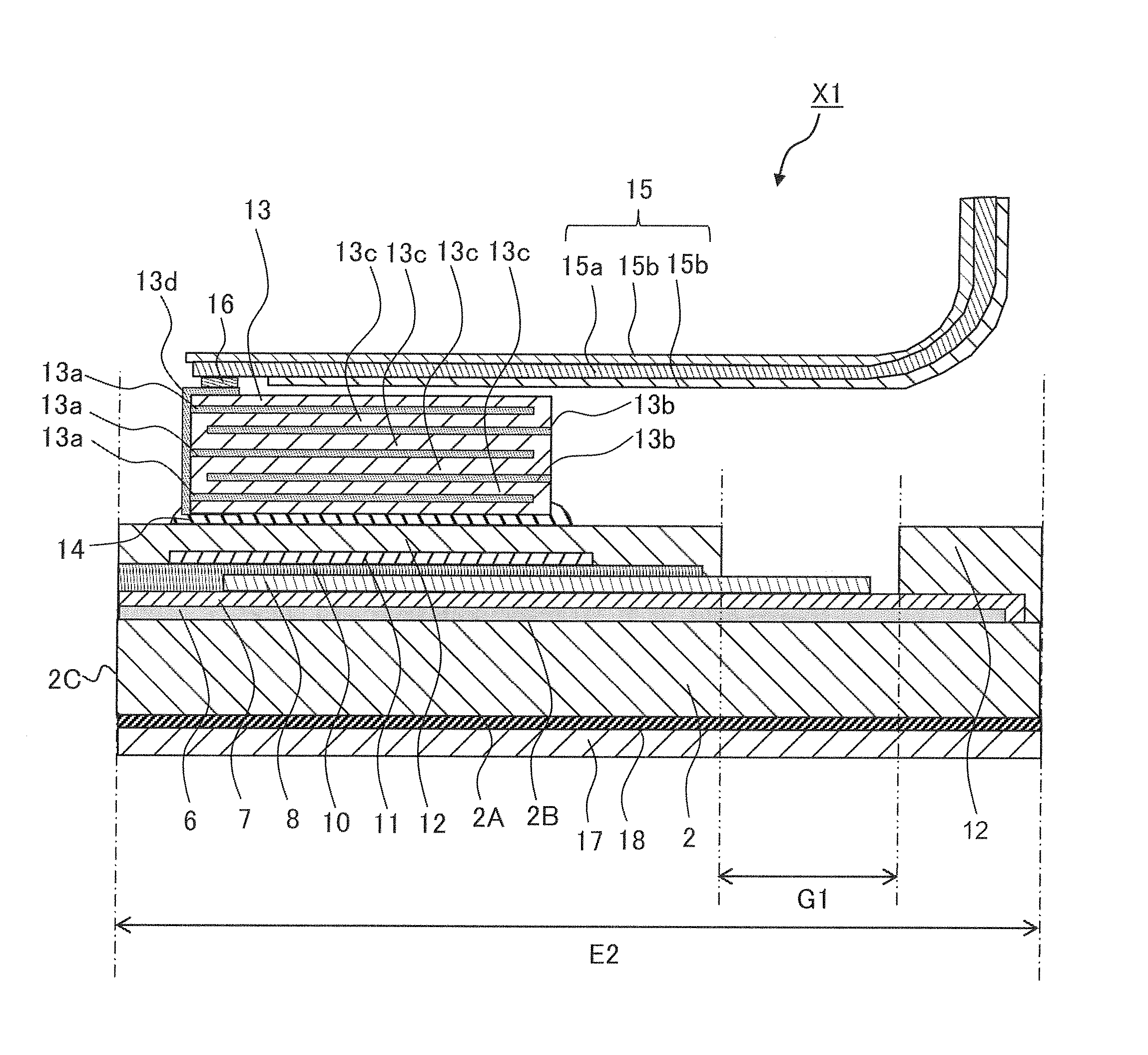
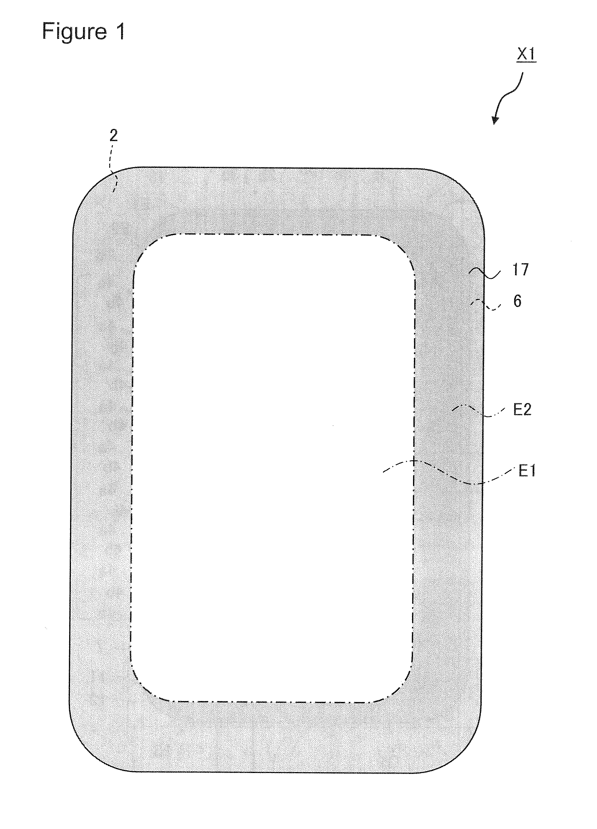
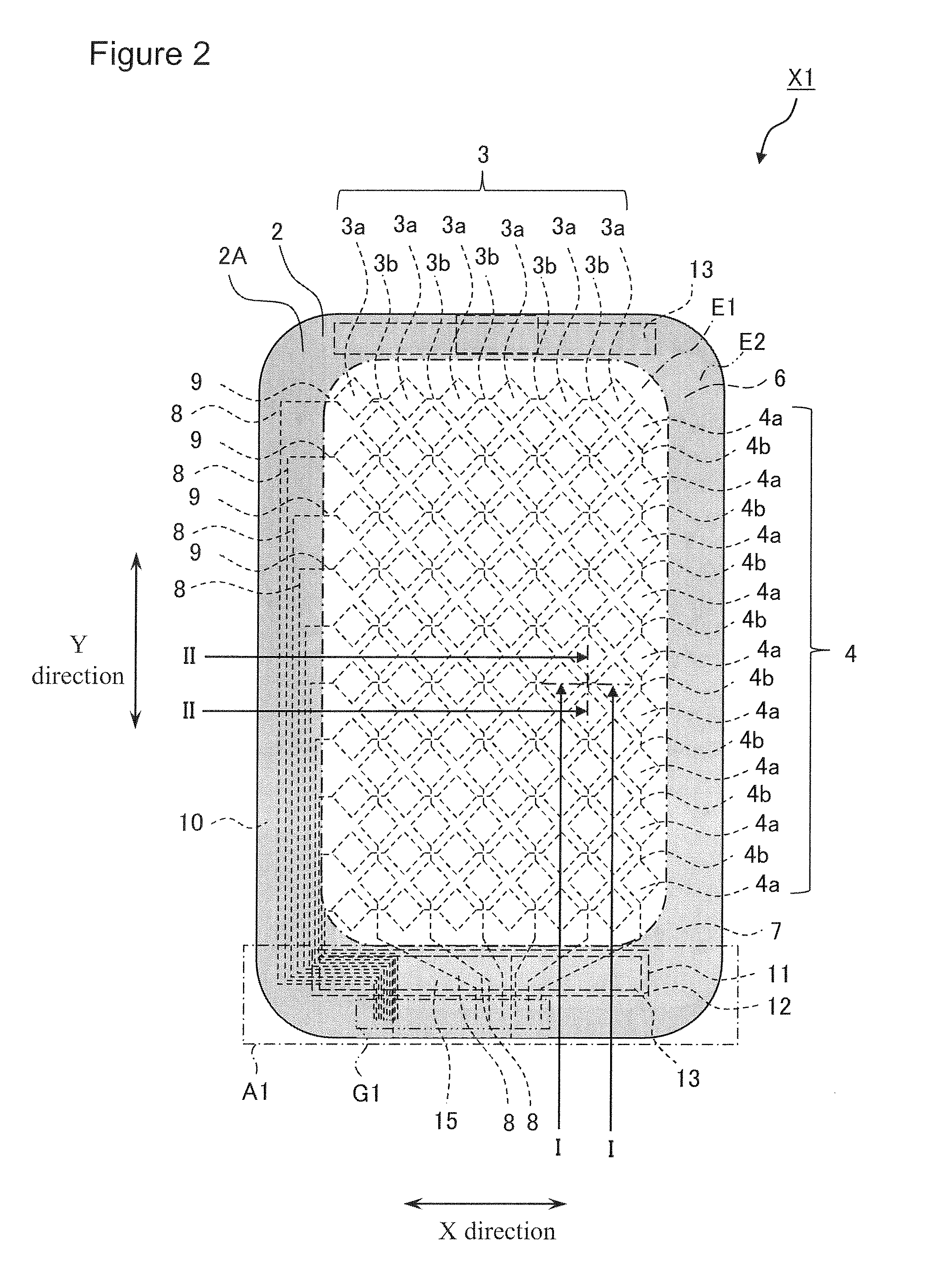
[0034]An input device X1 according to present embodiment is a projection type capacitive touch panel, as illustrated in FIGS. 1 and 2. The input device X1 includes an input area E1 and a non-input area E2. The input area E1 is an area in which a user can perform an input operation. The non-input area E2 is an area in which the user cannot perform an input operation. The non-input area E2 according to the present embodiment is located on the outer side of the input area E1 to surround the input area E1, but the invention is not limited thereto. For example, the non-input area E2 may be located within the input area E1.
[0035]In addition, the input device X1 is not limited to the projection type capacitive touch panel and may be, for example, a surface capacitive touch panel or a resistive film type touch panel.
[0036]The input device X1 includes a base 2, as illustrated in FIGS. 1 to 4. In addition, for convenience of description, an insulator 5, an adhesive member 14, a conductive adh...
embodiment 2
[0082]FIG. 11 is a plan view illustrating a schematic configuration of an input device X2 according to Embodiment 2 and is a view seen through a base 2. FIG. 12 is a plan view of an enlarged area B1 surrounded by a dash-dot line illustrated in FIG. 11 and is a view seen through from a second main surface 2B side of the base 2. FIG. 13 is a cross-sectional view taken along the line V-V illustrated in FIG. 12. In addition, in FIGS. 11 to 13, configurations having the same functions as those in FIGS. 2, 5, and 6 are denoted with the same reference signs and a detailed description thereof will be omitted.
[0083]The input device X2 further includes a second conductive layer 21, as illustrated in FIGS. 11 to 13. The second conductive layer 21 is provided on a covering layer 15b of a wiring board 15. In addition, a portion of the second conductive layer 21 is located between detection wires 8 and control wires 15a. Therefore, it is possible to reduce a possibility of electrical noise from t...
embodiment 3
[0086]FIG. 14 is a plan view illustrating a schematic configuration of an input device X3 according to Embodiment 3 and is a view seen through a base 2. FIG. 15 is a plan view of an enlarged area C1 surrounded by a dash-dot line illustrated in FIG. 14 and is a view seen through from a second main surface 2B side of the base 2. In addition, in FIGS. 14 and 15, configurations having the same functions as those in FIGS. 2 and 5 are denoted with the same reference signs and a detailed description thereof will be omitted.
[0087]The input device X3 includes detection wires 31 in place of the detection wires 8 included in the input device X1, as illustrated in FIGS. 14 and 15. The detection wires 31 are located on a first protective layer 7. In addition, ends of the detection wires 8 are electrically connected to connection wires 9, and the other ends of the detection wires 8 are located in an external conduction area G1. Here, the detection wires 8 do not overlap control wires 15a when vie...
PUM
 Abstract
Description
Claims
Application Information
 - R&D
- Intellectual Property
- Life Sciences
- Materials
- Tech Scout
- Unparalleled Data Quality
- Higher Quality Content
- 60% Fewer Hallucinations
Browse by: Latest US Patents, China's latest patents, Technical Efficacy Thesaurus, Application Domain, Technology Topic, Popular Technical Reports.
© 2025 PatSnap. All rights reserved.Legal|Privacy policy|Modern Slavery Act Transparency Statement|Sitemap|About US| Contact US: help@patsnap.com