Memory system

a memory system and memory technology, applied in the field of memory systems, can solve the problems of increasing current and increasing the area of the circuit, and achieve the effect of increasing the bandwidth, without increasing the area of the input/output-related circui

Inactive Publication Date: 2015-03-05
SK HYNIX INC
View PDF5 Cites 4 Cited by
  • Summary
  • Abstract
  • Description
  • Claims
  • Application Information

AI Technical Summary

Problems solved by technology

However, increasing a prefetch value causes an increase in an input / output-related circuit construction, such as local I / O, global I / O, and the like, thereby increasing current and increasing the area of the circuit.
Increasing an I / O width also causes the same problems.

Method used


Image

  • Memory system
  • Memory system
  • Memory system

Examples


Embodiment Construction

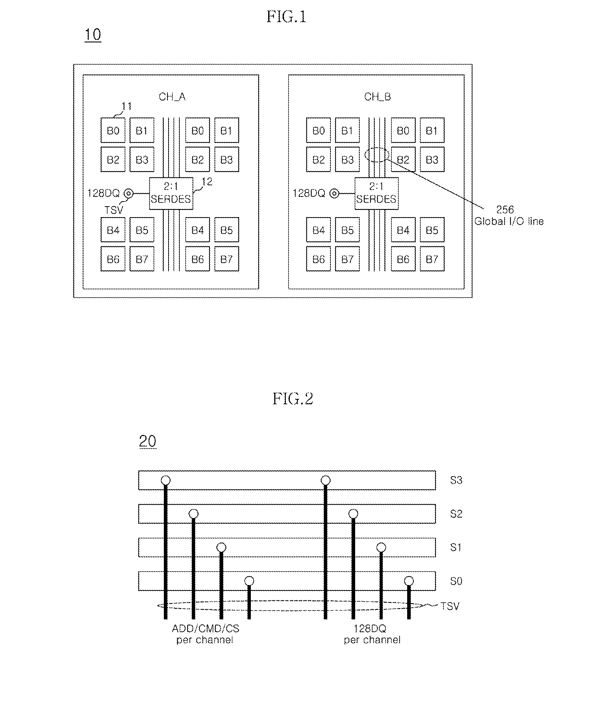
[0037]Hereinafter, a memory system according to the invention will be described below with reference to the accompanying drawings through various embodiments.

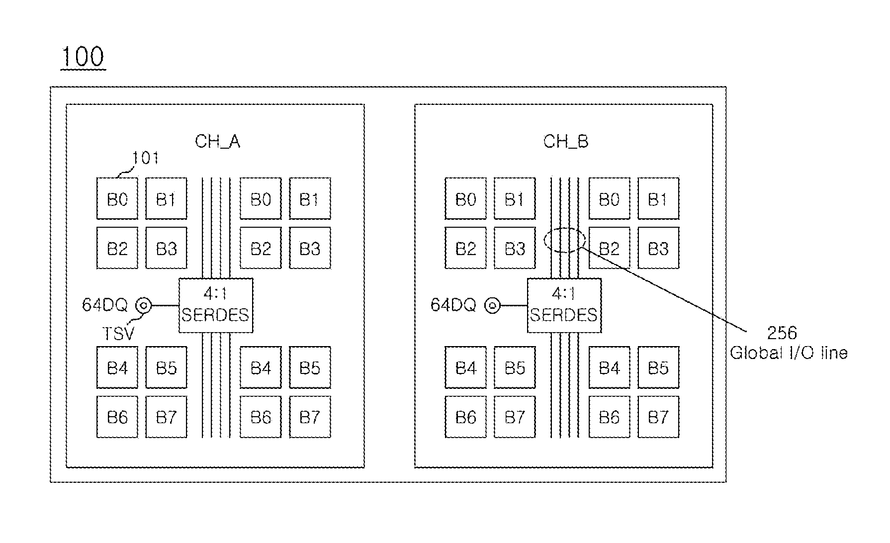
[0038]FIG. 4 is a layout diagram illustrating the configuration of a semiconductor memory chip 100 according to an embodiment of the invention.

[0039]As illustrated in FIG. 4, a semiconductor memory chip 100 according to an embodiment of the invention may be configured with two channels CH_A and CH_B, wherein each channel may include a plurality of memory banks 101 illustrated by B0-B3, a plurality of global I / O lines electrically coupled to the plurality of memory banks 101, a plurality of serializer / deserializers SERDES electrically coupled the plurality of global I / O lines, and a via (e.g. a through silicon via (TSV)).

[0040]In this case, the memory chip 100 may be called a slice in a stacked structure.

[0041]Each slice may include global I / O lines (e.g. 256 global I / O lines), data input / output terminals (e.g. 64 DQs), a serial...


PUM


Abstract

A memory system, including a plurality of stacked slices and a controller electrically coupled to the plurality of slices, includes: the plurality of slices configured to share a command in a preset number unit, wherein a slice performs a data input / output operation; and the controller configured to generate the command and a control signal for selecting slices in the preset number unit from the plurality of slices.

Description

CROSS-REFERENCES TO RELATED APPLICATION[0001]The present application claims priority under 35 U.S.C. §119(a) to Korean application number 10-2013-0103769, filed on Aug. 30, 2013, in the Korean Intellectual Property Office, which is incorporated herein by reference in its entirety.BACKGROUND[0002]1. Technical Field[0003]Various embodiments relate to a semiconductor circuit, and more particularly, to a memory system.[0004]2. Description of the Related Art[0005]A conventional memory chip can be configured with a single channel or with two channels which operate independently from each other.[0006]FIG. 1 is a layout diagram illustrating the configuration of a conventional semiconductor memory chip 10.[0007]As shown in FIG. 1, a conventional semiconductor memory chip 10 is configured, for example, with two channels CH_A and CH_B, wherein each channel includes a plurality of memory banks 11, a plurality of global I / O lines, a serializer / deserializer SERDES 12, and a through silicon via (T...

Claims


Application Information

Patent Timeline
Patent Type & Authority Applications(United States)
IPC IPC(8): G06F3/06
CPCG06F3/0659G06F3/0683G06F3/0604G11C5/025G11C7/10G11C7/1018G11C2207/107G11C2207/2272G11C7/00
Inventor LEE, DONG UK
Owner SK HYNIX INC
Why Eureka
Try Eureka