Millimetre wave integrated circuits with thin film transistors

a technology of integrated circuits and thin film transistors, which is applied in the direction of semiconductor devices, electrical equipment, capacitors, etc., can solve the problems of high toxic ions and complexes of arsenic, not only not required but also sometimes detrimental, and achieve the elimination or minimization of requirements for die or chip attachment, alignment and wire bonding.

Active Publication Date: 2015-03-12
SHIH ISHIANG +3
View PDF5 Cites 11 Cited by
  • Summary
  • Abstract
  • Description
  • Claims
  • Application Information

AI Technical Summary

Benefits of technology

[0007]One objective of the invention is to provide MMIC circuits without the needs of grinding and etching of the substrate after active and passive component fabrication. Another objective of the invention is to provide technology for active devices in a MMIC with...

Problems solved by technology

These bubbles or voids can increase the thermal resistance between the chip and carrier, hence lead to non-uniformity in the heat dissipation of heat from the chip during the operation.
On the other hand, for passive components such as transmission lines, capacitors and inductors, the presence of epitaxial layers and the associated semiconductor substrate is not only not required but also sometimes detrimental...

Method used


Image

  • Millimetre wave integrated circuits with thin film transistors
  • Millimetre wave integrated circuits with thin film transistors
  • Millimetre wave integrated circuits with thin film transistors

Examples


Embodiment Construction

1. Thin Film Transistor with a Flat Gate

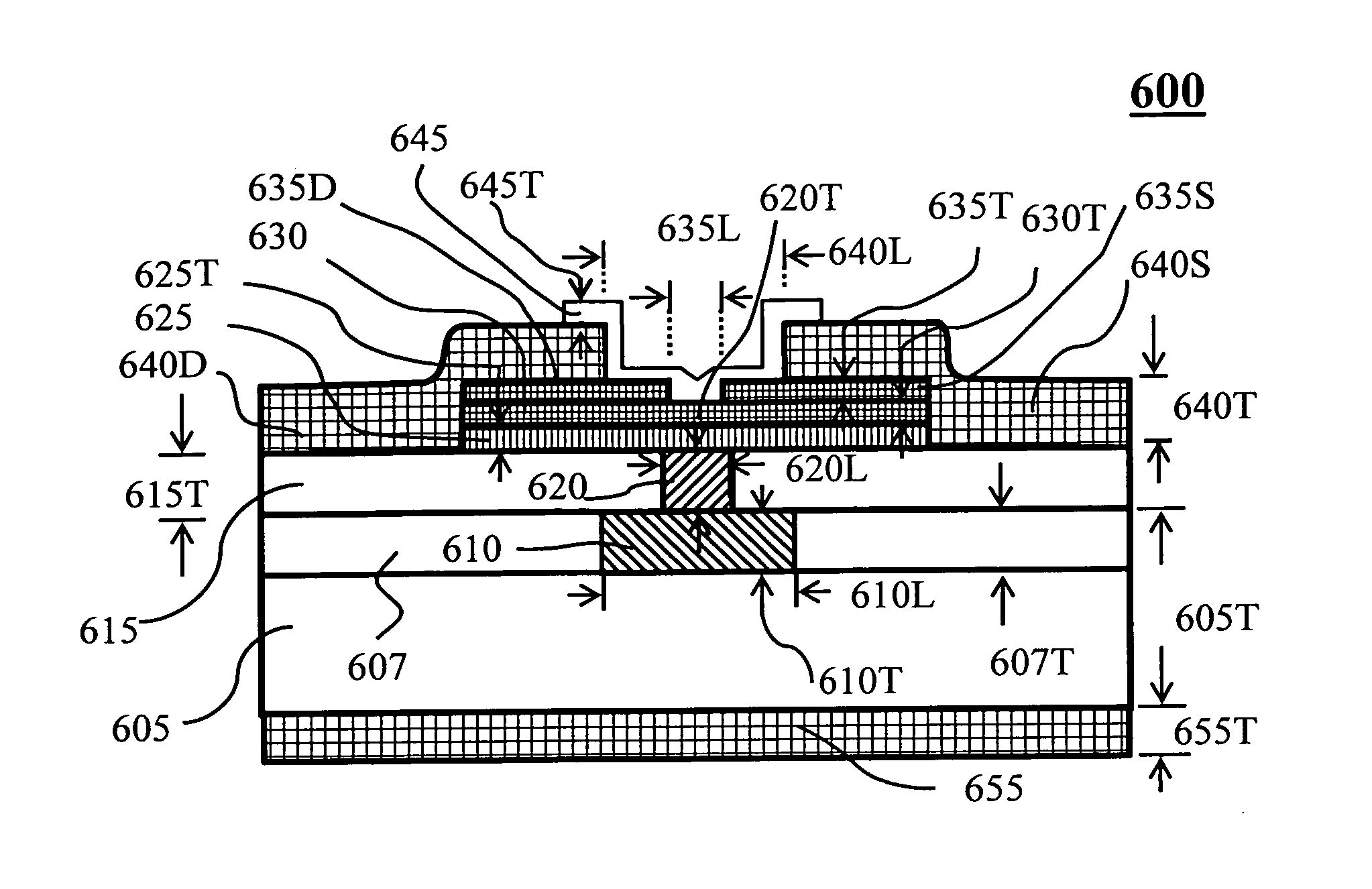
[0021]According to the present invention, a thin film transistor (100, FIG. 4) for microwave and millimetre wave integrated circuits (MMICs), comprises a dielectric substrate (105) with a substrate thickness (105T); a first metal gate (110) having a first metal gate thickness (110T) and a first metal gate length (110L); a first dielectric layer (115) with a first dielectric layer thickness (115T); a first semiconductor channel layer (120) with a first semiconductor channel layer thickness (120T) overlapping first metal gate (110) of its entire length (110L); a drain (125D) and a source (125S) having a drain / source thickness of (125T) and a source drain gap (125L); and a second dielectric layer (130) having a second dielectric layer thickness (130T) for protection and passivation.

[0022]According to this invention, material for the semiconductor channel layer (120) is selected to have high carrier mobility and a large breakdown electric field wh...


PUM


Abstract

MMIC circuits with thin film transistors are provided without the need of grinding and etching of the substrate after the fabrication of active and passive components. Furthermore, technology for active devices based on non-toxic compound semiconductors is provided. The success in the MMIC methods and structures without substrate grinding/etching and the use of semiconductors without toxic elements for active components will reduce manufacturing time, decrease economic cost and environmental burden. MMIC structures are provided where the requirements for die or chip attachment, alignment and wire bonding are eliminated completely or minimized. This will increase the reproducibility and reduce the manufacturing time for the MMIC circuits and modules.

Description

FIELD OF INVENTION[0001]This invention relates to millimetre wave devices and circuits with thin film transistors. Specifically, it relates to thin film transistors with high charge carrier mobility and large breakdown electric field.BACKGROUND OF THE INVENTION[0002]MMICs are important components for communication systems. This is especially true for wireless systems. Each of the wireless systems requires a transmitting and receiving (T / R) module to send or to receive microwave signals. As shown in FIG. 1, a typical T / R module has a first input matching circuit, a power amplifier (PA) and a first output matching circuit, a switch (SW) and an antenna for transmitting operation. A second input matching circuit, a low noise amplifier (LNA) and a second output matching circuit together with the switch are used for receiving operation. Power supply to PA and LNA, operation conditions and control of PA and LNA are achieved by a bias and control logic (BCL) circuit. The bias and control lo...

Claims


Application Information

Patent Timeline
IPC IPC(8): H01L27/13H01L21/84
CPCH01L21/84H01L27/13H01L27/1259H01L21/02565H01L21/47573H01L21/47635H01L27/1218H01L27/1225H01L27/124H01L27/1255H01L28/20H01L28/40H01L29/24H01L29/42384H01L29/66969
Inventor SHIH, ISHIANGQIU, CINDY X.QIU, CHUNONGSHIH, YI-CHI
Owner SHIH ISHIANG
Why Eureka
Try Eureka