Display device and method for manufacturing the same

a technology for a display device and a manufacturing method, applied in the field of display devices, can solve problems such as unsatisfactory productivity, and achieve the effects of increasing the screen area, reducing the adverse effects of recessed and protruding parts formed by thick wires, and low electrical resistance of wiring

Active Publication Date: 2015-03-12
PANASONIC INTELLECTUAL PROPERTY MANAGEMENT CO LTD
View PDF7 Cites 3 Cited by
  • Summary
  • Abstract
  • Description
  • Claims
  • Application Information

AI Technical Summary

Benefits of technology

[0008]According to this disclosure, a display device that addresses various issues associated with the increase in screen size is provided. In particular, since a thick wire is used, the electrical resistance of wiring is low, and, since the thick wire is embedded in the wire embedded layer, the adverse effects associated with recessed and protruding parts formed by the thick wire are ...

Problems solved by technology

According to such a method for manufacturing a display device, produc...

Method used


Image

  • Display device and method for manufacturing the same
  • Display device and method for manufacturing the same
  • Display device and method for manufacturing the same

Examples


Embodiment Construction

[0027]Embodiments of this disclosure will now be described with reference to the drawings.

[0028]The issues are found to be as follows.

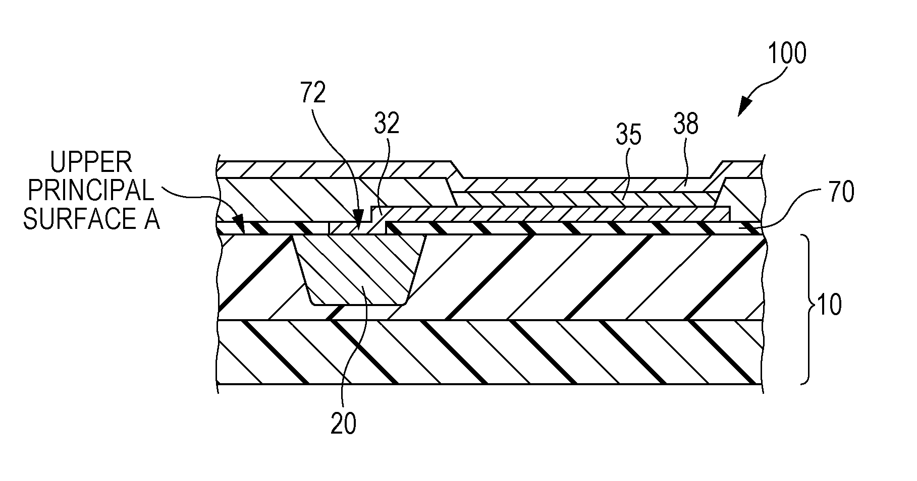
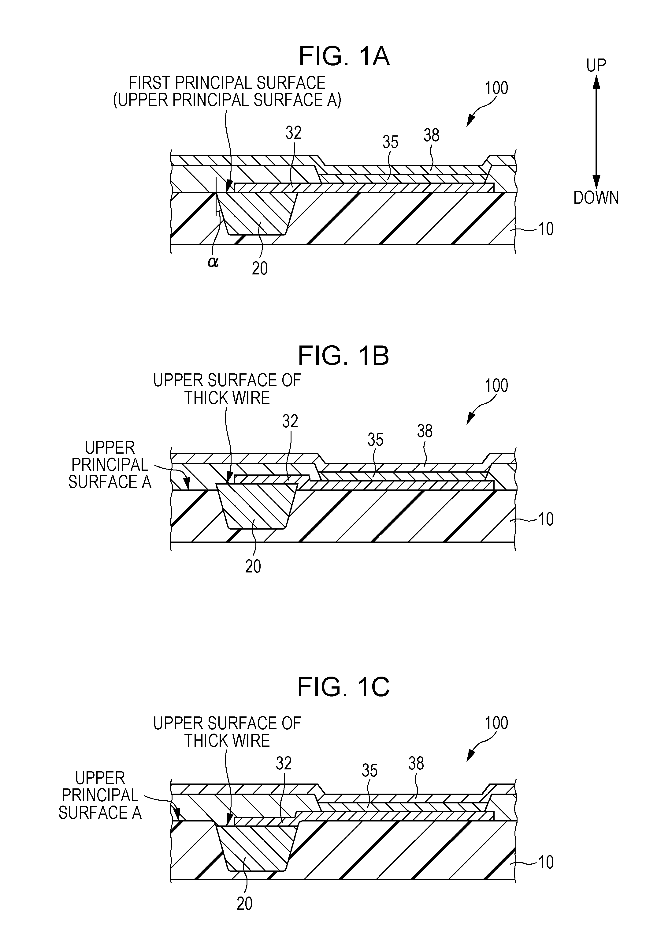
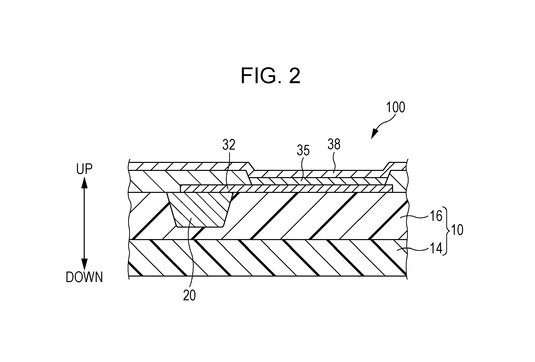
[0029]First, voltage reduction caused by wiring resistance becomes increasingly severe as the screen size (area) of display devices increases. Although voltage reduction can be decreased by increasing the thickness of the wire, a long process time will be needed to form thick wires by a vacuum process, resulting in lower productivity.

[0030]Second, forming thick wires causes the substrate to have protruding parts and recessed parts. A thick planarizing layer needs to be formed in order to form an OLED or the like on the substrate having protruding and recessed parts and thus the productivity is low.

[0031]Third, to address issues related to the protruding and recessed parts on the substrate, a wire structure formed by filling grooves formed in a glass substrate with a metal has been suggested (for example, refer to Japanese Unexamined Patent Application...


PUM


Abstract

A flexible display device includes a wire embedded layer that has flexibility and has a first principal surface, a thick wire embedded in the wire embedded layer so as to be substantially flush with the first principal surface of the wire embedded layer, an extraction lower electrode electrically connected to the thick wire and disposed on the first principal surface of the wire embedded layer, an emitting layer disposed on the extraction lower electrode, and an upper electrode disposed on the emitting layer. The flexible display device is suitable for large-screen devices and offers high productivity.

Description

BACKGROUND[0001]1. Field[0002]This disclosure relates to a display device and a method for manufacturing the display device. In particular, it relates to a passive-type display device and a method for manufacturing the passive-type display device.[0003]2. Description of the Related Art[0004]In recent years, various types of flat panel displays have been developed. Generally, a flat panel display includes a display medium constituted by elements that use liquid crystals, organic electroluminescence (EL), electrophoresis, or the like.[0005]A display device is manufactured by forming thin-film wires by vacuum process (for example, sputtering) and photolithography on an insulating substrate such as glass and then forming an image displaying unit such as a liquid crystal display (LCD) on the substrate and the thin-film wires.[0006]According to such a method for manufacturing a display device, productivity is not satisfactory if a large-screen display device is to be formed.SUMMARY[0007]A...

Claims


Application Information

Patent Timeline
IPC IPC(8): H05B33/06H05B33/10H05B33/12
CPCH05B33/06H05B33/10H05B33/12Y02E10/549Y02P70/50H10K59/1795H10K85/321H10K77/111H10K50/814H10K50/824H10K59/1201H10K71/00H10K59/00G09F9/30
Inventor SUZUKI, TAKESHITOMITA, YOSHIHIROHIRANO, KOICHIARAI, YASUHIRO
Owner PANASONIC INTELLECTUAL PROPERTY MANAGEMENT CO LTD
Why Eureka
Try Eureka