Semiconductor structure and device and methods of forming same using selective epitaxial process

a technology of epitaxial process and semiconductor, applied in the direction of semiconductor devices, electrical equipment, transistors, etc., can solve the problems of increasing the idle power requirements of the device, increasing the switching speed, and reducing the operating power consumption

Active Publication Date: 2015-04-02
ASM IP HLDG BV
View PDF1 Cites 372 Cited by
  • Summary
  • Abstract
  • Description
  • Claims
  • Application Information

AI Technical Summary

Benefits of technology

[0005]Various embodiments of the present disclosure relate to semiconductor structures and devices and to methods of forming the structures and device. More particularly, the disclosure relates to multi-gate or FinFET structures and devices and to methods of forming the same. While the ways in which

Problems solved by technology

The leakage, in turn, increase idle power requirements for the device.
The reduced leakage current not only reduces power consumption when the device is in an off state, but can also reduce a threshold voltage of the device, which can lead to increased switching speeds and reduced operating power consumption.
Unfortunately, inclusion of germanium in the channel region

Method used


Image

  • Semiconductor structure and device and methods of forming same using selective epitaxial process
  • Semiconductor structure and device and methods of forming same using selective epitaxial process
  • Semiconductor structure and device and methods of forming same using selective epitaxial process

Examples


Embodiment Construction

[0026]The description of exemplary embodiments of methods, structures, and devices provided below is merely exemplary and is intended for purposes of illustration only; the following description is not intended to limit the scope of the disclosure or the claims. Moreover, recitation of multiple embodiments having stated features is not intended to exclude other embodiments having additional features or other embodiments incorporating different combinations of the stated features.

[0027]The present disclosure relates, generally, to semiconductor devices and structures and to methods of forming the devices as structures. As set forth in more detail below, the structure may be used to form devices including multiple gates, such as FinFET devices, having germanium in the channel region.

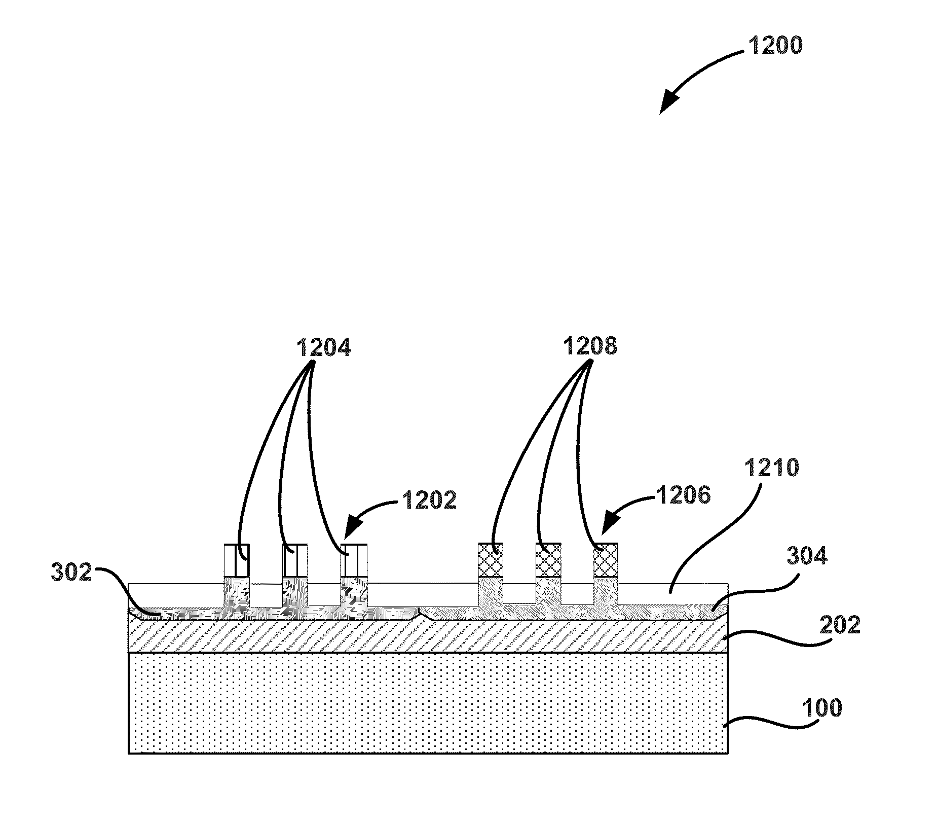
[0028]FIG. 12 illustrates a structure 1200 in accordance with exemplary embodiments of the disclosure and FIGS. 1-11 illustrate structures formed during the fabrication of structure 1200. Structure 1200 is...


PUM


Abstract

Semiconductor structures, devices, and methods of forming the structures and device are disclosed. Exemplary structures include multi-gate or FinFET structures that can include both re-channel MOS (NMOS) and p-channel MOS (PMOS) devices to form CMOS structures and devices on a substrate. The devices can be formed using selective epitaxy and shallow trench isolation techniques.

Description

FIELD OF INVENTION[0001]The present disclosure generally relates to semiconductor structures and devices. More particularly, the disclosure relates to semiconductor structures and devices including one or more layers formed using a selective epitaxial deposition process.BACKGROUND OF THE DISCLOSURE[0002]Multi-gate semiconductor devices, including and sometimes generally referred to as FinFET devices, have recently attracted more attention, because the devices offer higher performance per unit of power compared to similar, single gate / planar devices. With traditional metal oxide semiconductor (MOS) devices, as device geometries continue to shrink in an effort to increase performance of the device, short channel effects, such as off-state leakage current, increase. The leakage, in turn, increase idle power requirements for the device.[0003]FinFET devices include a gate structure that can mitigate leakage current. The reduced leakage current not only reduces power consumption when the ...

Claims


Application Information

Patent Timeline
IPC IPC(8): H01L27/092H01L21/8238
CPCH01L21/823821H01L27/0924H01L29/7831H01L29/785H01L27/0928H01L29/0649H01L29/165
Inventor XIE, QIMACHKAOUTSAN, VLADIMIRMAES, JAN WILLEM
Owner ASM IP HLDG BV
Why Eureka
Try Eureka