Semiconductor memory apparatus and data input and output method thereof

a semiconductor memory and data input technology, applied in the direction of digital storage, input/output of record carriers, instruments, etc., can solve the problems of noise generation, misoperation, and likely deterioration of the performance of the semiconductor memory apparatus

Inactive Publication Date: 2015-04-02
SK HYNIX INC
View PDF6 Cites 10 Cited by
  • Summary
  • Abstract
  • Description
  • Claims
  • Application Information

AI Technical Summary

Problems solved by technology

However, in the semiconductor memory apparatuses operating at a high frequency band, the performances of the semiconductor memory apparatuses are likely to deteriorate due to noise of data.
Nevertheless, problems are still caused in that noise is generated and misoperation occurs due to an increase in the number of data switching times in the high frequency band.
Nonetheless, in the conventional semiconductor memory apparatus, since whether to output the data by inverting or non-inverting (i.e. transmitting) them is determined and data may be inverted only in the data output unit 12, a problem is caused in that current consumption is substantial due to toggling of the data input / output lines for transmitting data.
Also, in the conventional art, due to an interfacing problem that is likely to occur between the semiconductor memory apparatus and the chipset, the inversion operation may be performed only in a DBI mode by receiving the mode signal ‘mode’ that is generated from the mode register set and cannot be performed in a normal mode.

Method used


Image

  • Semiconductor memory apparatus and data input and output method thereof
  • Semiconductor memory apparatus and data input and output method thereof
  • Semiconductor memory apparatus and data input and output method thereof

Examples


Embodiment Construction

[0020]Hereinafter, a semiconductor memory apparatus and a data input and output method thereof according to the present invention will be described below with reference to the accompanying drawings through various examples of embodiments.

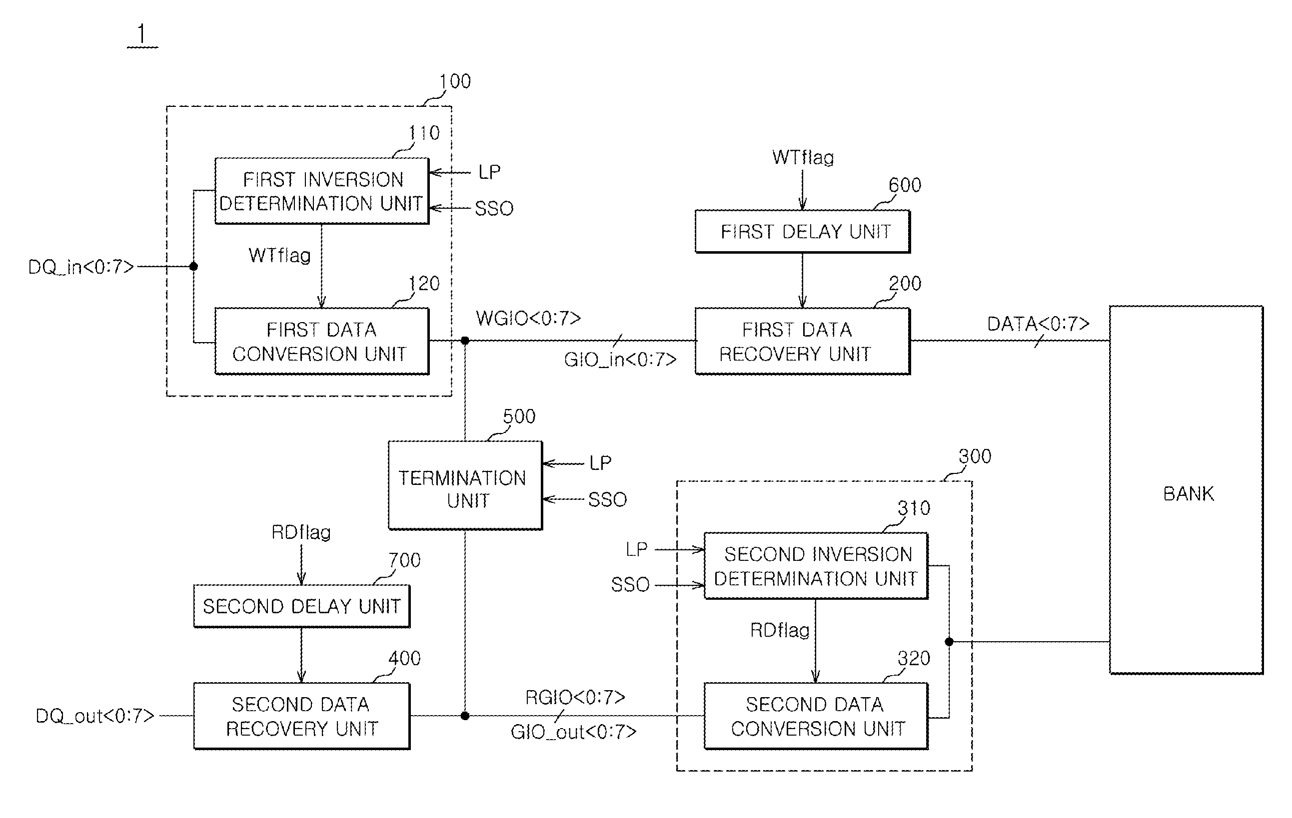
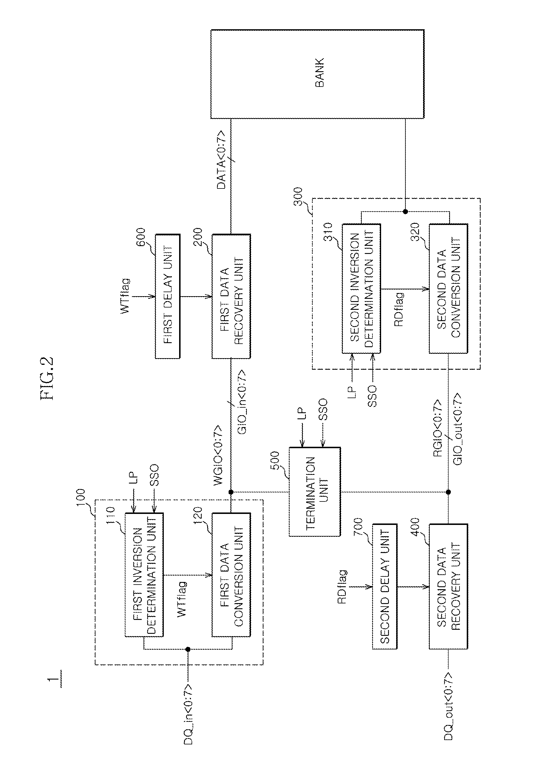
[0021]Referring to FIG. 2, a semiconductor memory apparatus 1 includes an input data bus inversion unit 100, data input lines WGIO, a first data recovery unit 200, a memory bank BANK, an output data bus inversion unit 300, data output lines RGIO, a second data recovery unit 400 and a termination unit 500.

[0022]When the data input operation of the semiconductor memory apparatus 1 is performed, a plurality of input data DQ_in are inputted to the semiconductor memory apparatus 1 from outside through data pads (not shown). The input data bus inversion unit 100 is configured to receive the plurality of input data DQ_in and determine whether or not to invert the plurality of input data DQ_in based on an operation mode signals LP and SSO and the plurality ...


PUM


Abstract

A semiconductor memory apparatus includes an input data bus inversion unit, a data input line, a termination unit, a data recovery unit and a memory bank. The input data bus inversion unit determines whether or not to invert a plurality of input data based on an operation mode signal and the plurality of input data and generates a plurality of conversion data. The data input line transmits the plurality of conversion data. The termination unit terminates the data input line in response to the operation mode signal. The data recovery unit receives the plurality of conversion data and generates a plurality of storage data. The memory bank configured to store the plurality of storage data.

Description

CROSS-REFERENCES TO RELATED APPLICATION[0001]The present application claims priority under 35 U.S.C. §119(a) to Korean application number 10-2013-0116283, filed on Sep. 30, 2013, in the Korean Intellectual Property Office, which is incorporated herein by reference in its entirety as set forth in full.BACKGROUND[0002]1. Technical Field[0003]Various embodiments relate to a semiconductor memory apparatus, and more particularly, to a semiconductor memory apparatus that adopts data bus inversion.[0004]2. Related Art[0005]As the data processing speeds of a central processing unit (CPU) and a graphic processing unit (GPU) are gradually increased, semiconductor memory apparatuses capable of operating at a high frequency are needed inevitably. However, in the semiconductor memory apparatuses operating at a high frequency band, the performances of the semiconductor memory apparatuses are likely to deteriorate due to noise of data. In order to solve this problem, the strength of a data driver ...

Claims


Application Information

Patent Timeline
Patent Type & Authority Applications(United States)
IPC IPC(8): G06F3/06
CPCG06F3/0661G06F2003/0697G06F3/0671G06F3/0614G06F13/4234G11C7/1006G11C7/10
Inventor KWACK, SEUNG WOOK
Owner SK HYNIX INC
Why Eureka
Try Eureka