Semiconductor device including a clock adjustment circuit

a technology of adjusting circuit and semiconductor device, which is applied in the direction of single output arrangement, pulse automatic control, electrical apparatus, etc., can solve the problems of affecting the initial operation time, relatively long time taken until the internal clock signal is locked,

Active Publication Date: 2015-04-09
MICRON TECH INC
View PDF12 Cites 13 Cited by
  • Summary
  • Abstract
  • Description
  • Claims
  • Application Information

AI Technical Summary

Problems solved by technology

In the DLL circuit, a time taken for an initial operation may be problematic.
This is because, in the initial operation, since the phase of an internal clock signal largely changes, a relatively long time is taken until the internal clock signal is locked.

Method used


Image

  • Semiconductor device including a clock adjustment circuit
  • Semiconductor device including a clock adjustment circuit
  • Semiconductor device including a clock adjustment circuit

Examples


Embodiment Construction

[0030]The invention will be now described herein with reference to illustrative embodiments. Those skilled in the art will recognize that many alternative embodiments can be realized using the teachings of the present invention and that the invention is not limited to the embodiments illustrated for explanatory purposes.

[0031]A first embodiment of the present invention will be described below in detail with reference to the accompanying drawings.

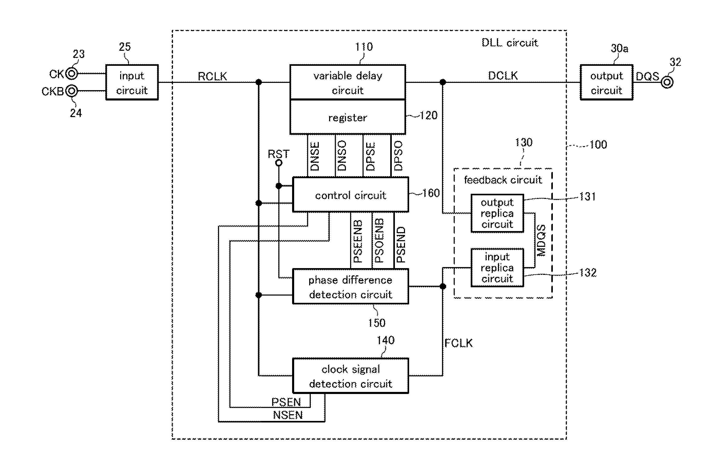
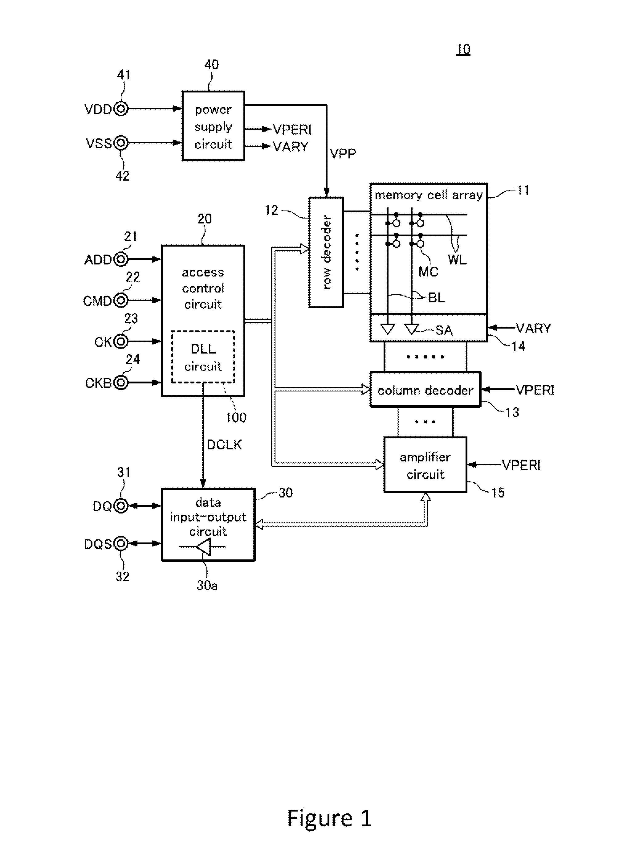
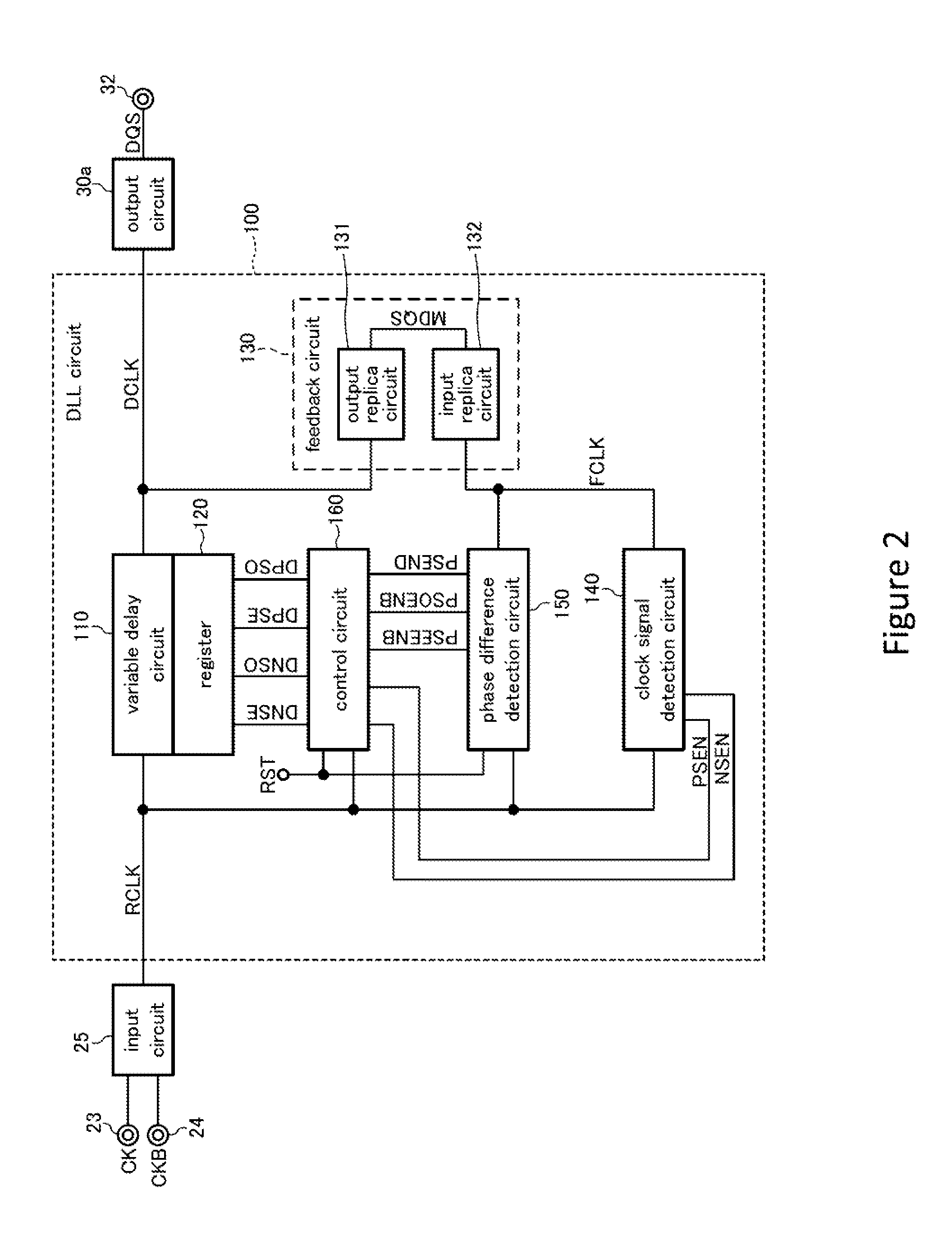
[0032]FIG. 1 is a block diagram showing an entire configuration of a semiconductor device 10 according to an embodiment of the present invention.

[0033]The semiconductor device 10 according to the embodiment is a DRAM, and includes a memory cell array 11 as shown in FIG. 1. In the memory cell array 11, a plurality of word lines WL and a plurality of bit lines BL are arranged, the word lines WL and the bit lines BL crossing each other, and memory cells MC are arranged at nodes between the word lines WL and the bit lines BL, respectively. Selec...


PUM


Abstract

Disclosed herein is a semiconductor device that includes a first circuit comprising a plurality of first logic elements coupled in cascade and configured, in response to first and second clock signals and a control signal, to produce control information that indicates a first number of the first logic elements through which the control signal has been propagated during a period defined by a first change in logic level of the first clock signal and by a second change in logic level of the second clock signal, the first and second changes occurring adjacently to each other in same directions as each other, and a second circuit comprising a delay circuit configured to receive the first clock signal and the control information and to produce a third clock signal by delaying the first clock signal by an amount responsive to the control information.

Description

RELATED REFERENCE[0001]This application is based upon and claims the benefit of priority from Japanese Patent Application No. 2013-211373 filed on Oct. 8, 2013, the disclosure of which is incorporated herein in its entirety by reference.BACKGROUND[0002]1. Field of the Invention[0003]The present invention relates to a semiconductor device and, more specifically, to a semiconductor device including a variable delay circuit to generate an internal clock signal.[0004]2. Description of Related Art[0005]A semiconductor device such as a DRAM (Dynamic Random Access Memory) may include a clock generating circuit that generates an internal clock signal controlled in phase. As a typical clock generating circuit, a DLL (Delay Locked Loop) circuit is known as a clock adjustment circuit. The DLL circuit has a variable delay circuit that delays an external clock signal to generate an internal clock signal.[0006]In the DLL circuit, a time taken for an initial operation may be problematic. This is b...

Claims


Application Information

Patent Timeline
Patent Type & Authority Applications(United States)
IPC IPC(8): H03L7/085H03K5/14
CPCH03K5/14H03L7/085H03L7/0814H03L7/0816H03L7/0812
Inventor TANIGUCHI, NOBUTAKA
Owner MICRON TECH INC
Why Eureka
Try Eureka