Polishing method

Active Publication Date: 2015-04-09
EBARA CORP
View PDF3 Cites 2 Cited by
  • Summary
  • Abstract
  • Description
  • Claims
  • Application Information

AI Technical Summary

Benefits of technology

[0007]According to an embodiment, there is provided a polishing method

Problems solved by technology

However, it is difficult to terminate the polishing process immediately at a point of time when a target thickness is actually reached.
This reason is that the film-thickness detection entails a detection delay time and that it takes a certain time to actually stop the polishing of the conducti

Method used


Image

  • Polishing method
  • Polishing method
  • Polishing method

Examples


Example

[0026]Embodiments will be described with reference to the drawings.

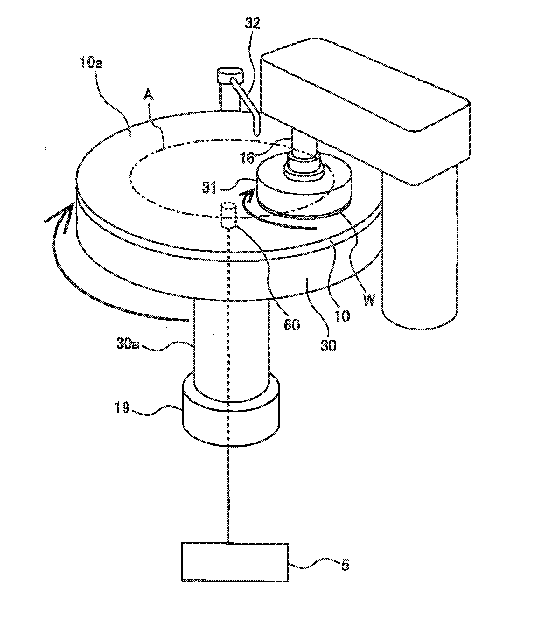
[0027]FIG. 1 is a perspective view schematically showing a polishing apparatus capable performing an embodiment of a polishing method according to an embodiment. As shown in FIG. 1, a polishing table 30 is coupled to a table motor 19 through a table shaft 30a, so that the polishing table 30 is rotated by the table motor 19 in a direction indicated by arrow. The table motor 19 is located below the polishing table 30. A polishing pad 10 is attached to an upper surface of the polishing table 30. The polishing pad 10 has an upper surface 10a, which provides a polishing surface for polishing a substrate W, such as a wafer. A top ring 31 is secured to a lower end of a top ring shaft 16. The top ring 31 is configured to hold the wafer W on its lower surface by vacuum suction. The top ring shaft 16 is elevated and lowered by an elevating mechanism (not shown in the drawing).

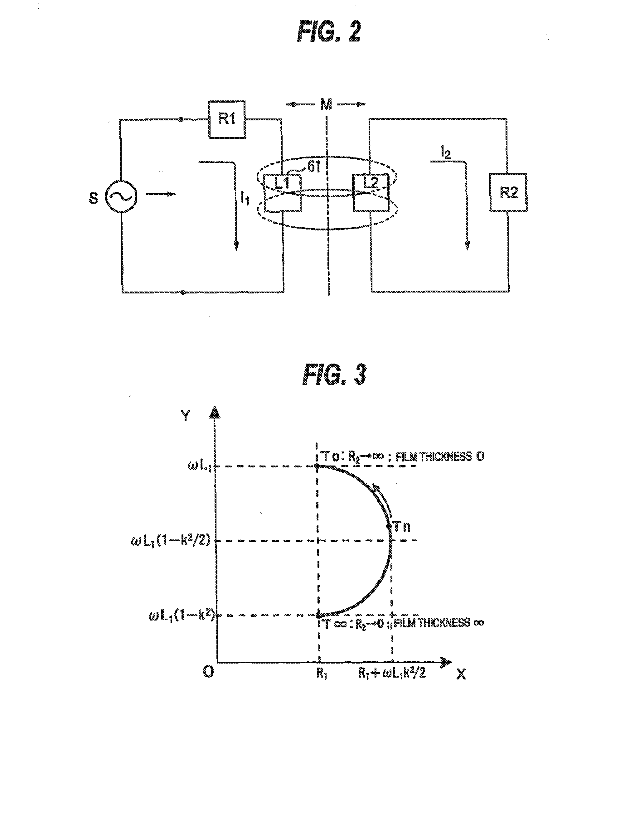
[0028]An eddy current film-thickness sensor 60 for ...


PUM


Abstract

A polishing method includes: rotating a polishing table that supports a polishing pad; polishing a conductive film by pressing a substrate having the conductive film against the polishing pad; obtaining a film thickness signal with use of an eddy current film-thickness sensor disposed in the polishing table; determining a thickness of the polishing pad based on the film thickness signal; determining a polishing rate of the conductive film corresponding to the determined thickness of the polishing pad; calculating an expected amount of polishing of the conductive film to be polished at the determined polishing rate for a predetermined polishing time; calculating a temporary end-point film thickness by adding the expected amount of polishing to a target thickness; and terminating polishing of the conductive film when the predetermined polishing time has elapsed from a point of time when the thickness of the conductive film has reached the temporary end-point film thickness.

Description

CROSS REFERENCE TO RELATED APPLICATION[0001]This document claims priority to Japanese Patent Application Number 2013-210387 filed Oct. 7, 2013, the entire contents of which am hereby incorporated by reference.BACKGROUND[0002]In fabrication of semiconductor devices, a process of polishing a conductive film, such as a metal film, formed on a substrate is performed. For example, in a metal interconnect forming process, the metal film is formed on a surface of the substrate having interconnect patterns formed thereon and then chemical mechanical polishing (CMP) is performed to remove an excessive metal film, thereby forming metal interconnects. In this polishing process, in order to detect a polishing end point at which a desired target thickness is reached, an eddy current film-thickness sensor is used to measure the thickness of the conductive film formed on the substrate (see Japanese laid-open patent publication No. 2005-121616).[0003]The eddy current film-thickness sensor is dispos...

Claims


Application Information

Patent Timeline
IPC IPC(8): B24B49/18H01L21/304
CPCH01L21/304B24B49/18B24B37/013
Inventor TAKAHASHI, TAROKAWABATA, YASUMITSU
Owner EBARA CORP
Why Eureka
Try Eureka