Light-emitting device and electronic apparatus

Active Publication Date: 2015-04-16
SEIKO EPSON CORP
View PDF5 Cites 11 Cited by
  • Summary
  • Abstract
  • Description
  • Claims
  • Application Information

AI Technical Summary

Benefits of technology

[0008]An advantage of one or more embodiments disclosed herein is that sufficient sealing performance is secured while suppressing an increase in the complexity of a manufacturing process. In addition, an advant

Problems solved by technology

However, in the technique of JP-A-2006-147528, there is a possibility that moisture and outside air may infiltrate into the boundary portion between the side end surface of the sealing layer and a base surface where the sealing layer is formed (for example, the surface of the substrate) and may reach the light-emitting element.
However, since an additional process of forming the element that blocks the boundary portion between the sealing layer and the base surface needs to be included, there is a problem in that the manufacturing process becomes complex.
In addition, there may be cases where light is

Method used


Image

  • Light-emitting device and electronic apparatus
  • Light-emitting device and electronic apparatus
  • Light-emitting device and electronic apparatus

Examples


first embodiment

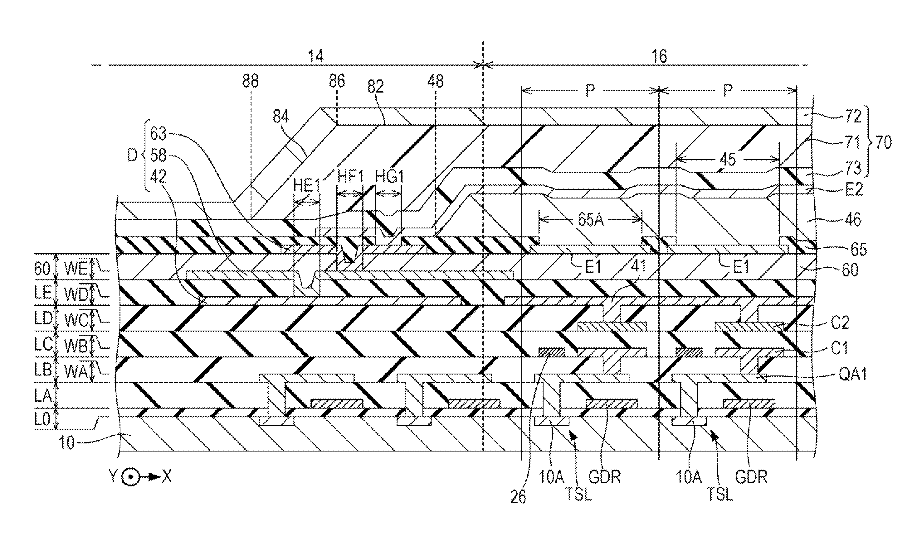
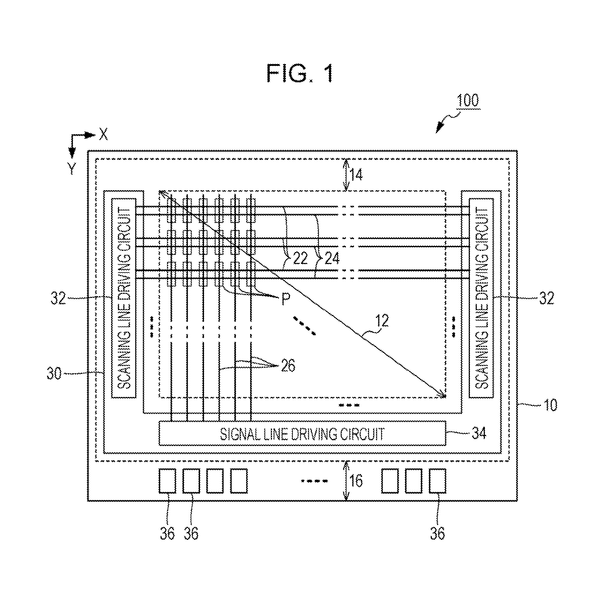
[0044]FIG. 1 is a plan view of a light-emitting device 100 according to a first embodiment. The light-emitting device 100 of the first embodiment is an organic EL device in which light-emitting elements that use an organic EL material are formed on the surface of a substrate 10. The substrate 10 is a plate-like member (semiconductor substrate) formed of a semiconductor material such as silicon and is used as a base body (base) on which a plurality of light-emitting elements are formed.

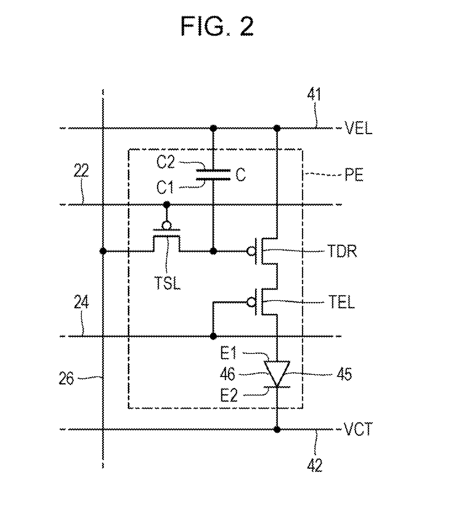
[0045]As exemplified in FIG. 1, a display region 12, a peripheral region 14, and a mounting region 16 are demarcated on the surface of the substrate 10. The display region 12 is a rectangular region in which a plurality of pixels P are arranged. In the display region 12, a plurality of scanning lines 22 that extend in an X direction, a plurality of control lines 24 that extend in the X direction to respectively correspond to the scanning lines 22, and a plurality of signal lines 26 that extend in a Y d...

second embodiment

[0103]A second embodiment will now be described. In the embodiments exemplified as follows, like elements having the same actions or functions as those of the first embodiment are denoted by like reference numerals referred to in the description of the first embodiment, and detailed description thereof will be appropriately omitted.

[0104]FIG. 19 is an explanatory view of the filter layer 90 formed on the surface of the sealing body 70 of the second embodiment. As exemplified in FIG. 19, in the insulating layer 92 of the second embodiment, the opening 92B described in the first embodiment is not formed. The protection portion 96 of the second embodiment is different from that of the first embodiment in the positional relationship between the peripheral edges of the layers (the first, second, and third layers 96R, 96G, and 96B). In the first embodiment, the peripheral edges of the layers of the protection portion 96 overlap each other in the plan view (the side surfaces of the layers ...

modification example

[0107]The embodiments discussed above may be modified in various forms. Specific modifications are described below. Two or more forms that are arbitrarily selected from the following examples may be appropriately combined.

[0108](1) From the viewpoint of reducing the height difference in the surface of the filter layer 90, as illustrated in FIG. 20, the protection portion 96 having the same film thickness as that of the insulating layer 92 may be formed on the inside of the opening 92B formed in the insulating layer 92. According to the above configuration, as illustrated in FIG. 20, since the surface of the insulating layer 92 and the surface of the protection portion 96 are positioned on substantially the same plane, an effect of a reduction in the height difference in the surface of the filter layer 90 becomes more significant.

[0109]However, in the case where the spin coating method or the like is employed to form the adhesive layer 21, there is a possibility that the adhesive tha...


PUM


Abstract

A light-emitting device includes a light-emitting element disposed in a display region and including a first electrode, a second electrode, and a light-emitting functional layer. The light-emitting device includes a wiring formed in a periphery of the display region and that is electrically connected to the second electrode, and a filter layer having a first color filter that overlaps the light-emitting element and a first layer that overlaps the peripheral wiring. The first color filter and the first layer are formed from a first colored layer that transmits light having a first wavelength.

Description

CROSS-REFERENCE TO RELATED APPLICATIONS[0001]This application claims benefit of Japanese Applications JP 2013-212403 and 2013-212404, both filed on Oct. 10, 2013. The disclosures of the prior applications are hereby incorporated by reference herein in their entirety.BACKGROUND[0002]1. Technical Field[0003]Various embodiments relate to a light-emitting device which uses a light-emitting material such as an organic electroluminescent (EL) material.[0004]2. Related Art[0005]A light-emitting device having light-emitting elements which use an organic EL material and are arranged on a display region of a substrate is hitherto suggested. The light-emitting element includes an anode electrode, a cathode electrode, and a light-emitting functional layer which emits light according to current between the two electrodes. A potential corresponding to the luminance for light emission is supplied to the anode electrode, and a lower power supply potential is supplied to the cathode electrode. In JP...

Claims


Application Information

Patent Timeline
IPC IPC(8): H01L27/32H01L51/52
CPCH01L27/322H01L51/5246H10K59/38H10K59/131H10K50/8426H10K59/123H10K59/124H10K59/126
Inventor TOYA, TAKASHIKOSHIHARA, TAKESHIKUBOTA, NAOTAKANOZAWA, RYOICHI
Owner SEIKO EPSON CORP
Why Eureka
Try Eureka