Image processing device, display device, electronic device and method for processing an image

a technology of image processing and display device, applied in the field of image processing device, display device, electronic device and image processing method, can solve problems such as degradation of display image, and achieve the effects of reducing power consumption, reducing luminance in the range, and reducing power consumption

Active Publication Date: 2015-04-23
JAPAN DISPLAY INC
View PDF3 Cites 17 Cited by
  • Summary
  • Abstract
  • Description
  • Claims
  • Application Information

AI Technical Summary

Benefits of technology

[0009]According to the invention, the luminance is decreased based on the relation between saturation and the luminance attenuation ratio. It enables to control the change of impression of a viewer to the display image in the human sense against colors. According to this invention, it enables to reduce the power consumption by decreasing luminance in the range without degrading the display image.

Problems solved by technology

In this case, it leads a degradation of the display image due to low luminance of a whole image or change of impression of a viewer.

Method used


Image

  • Image processing device, display device, electronic device and method for processing an image
  • Image processing device, display device, electronic device and method for processing an image
  • Image processing device, display device, electronic device and method for processing an image

Examples


first embodiment

[0054]A first embodiment is explained in detail below with reference to the accompanying drawings.

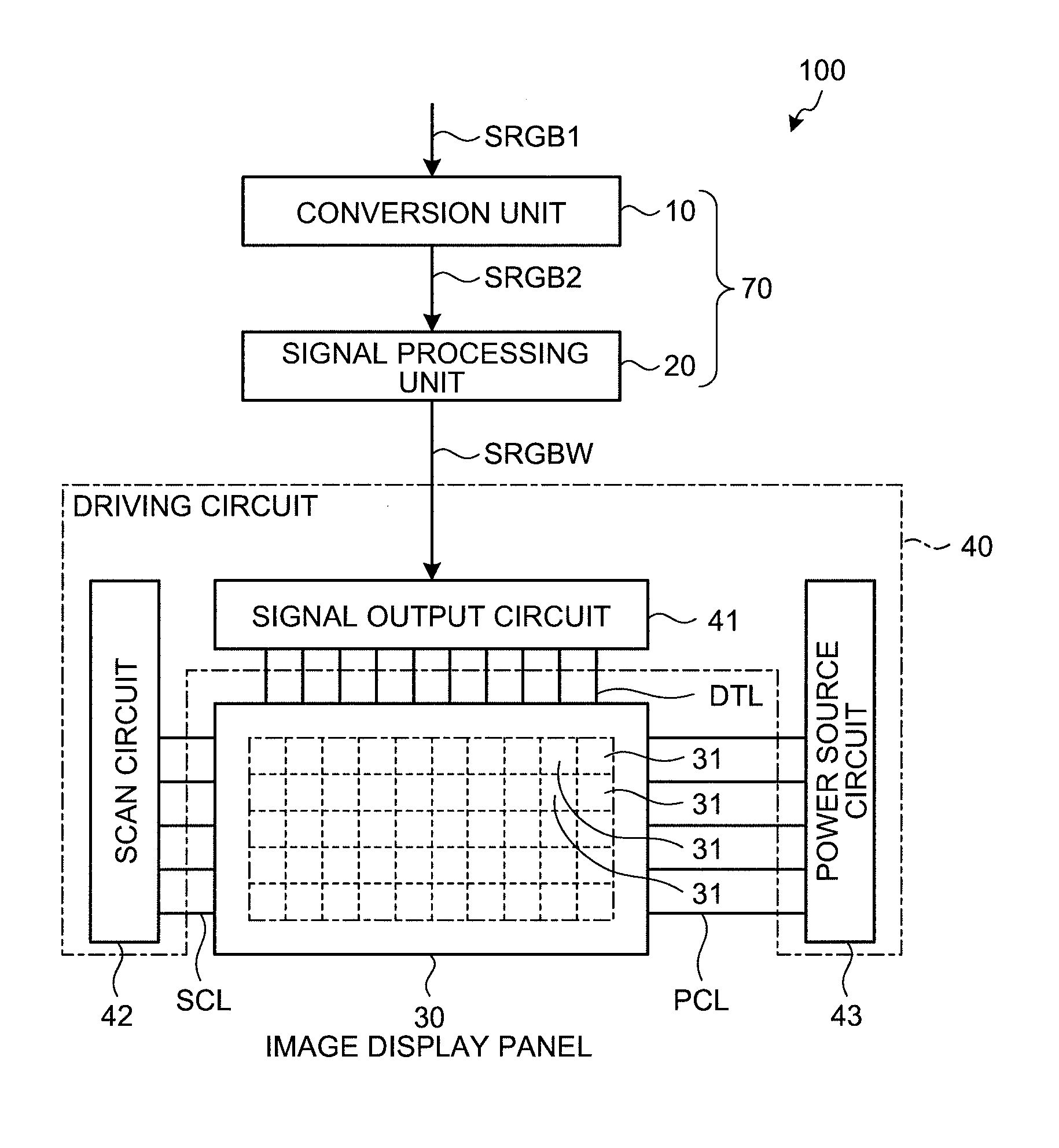
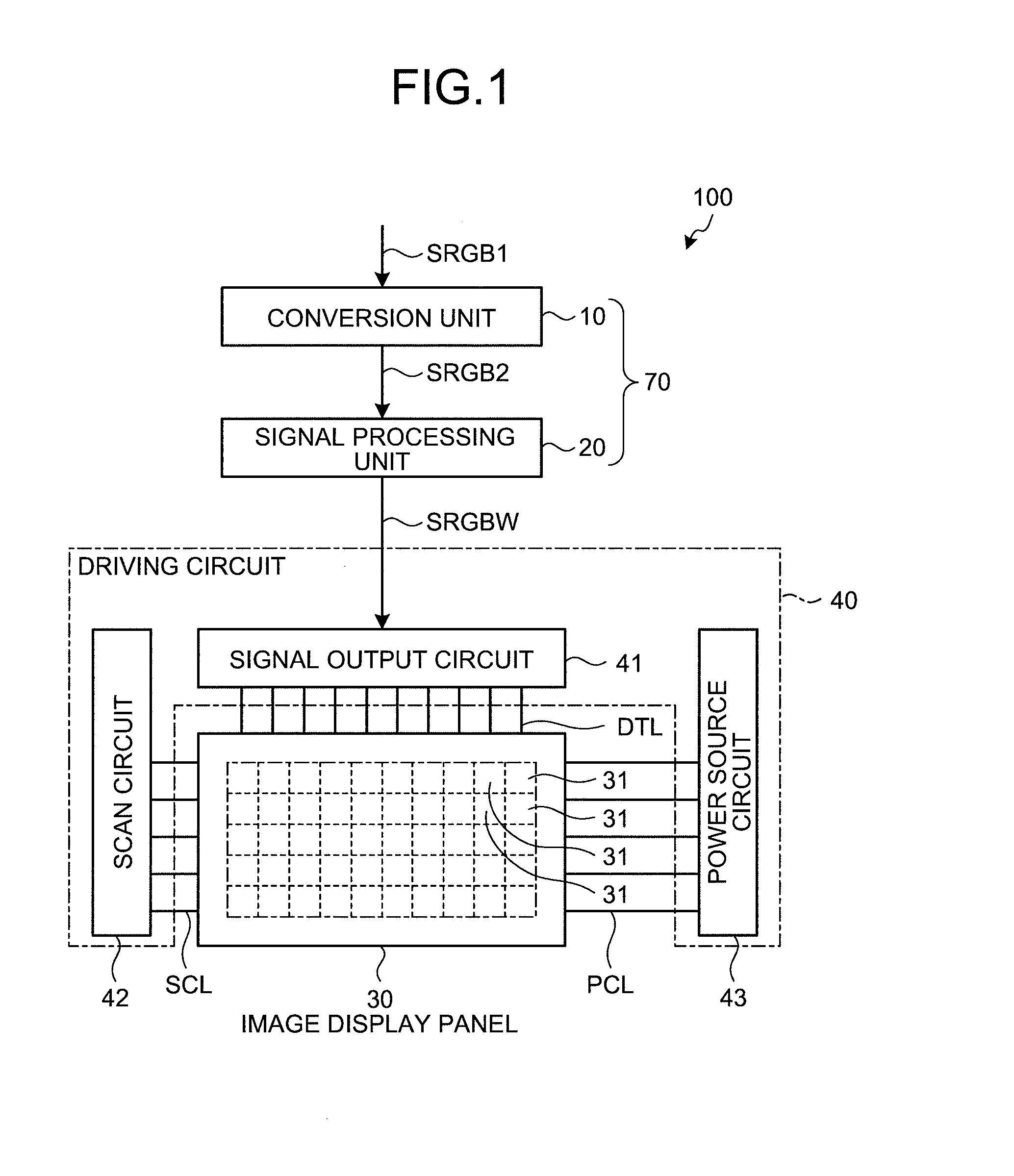
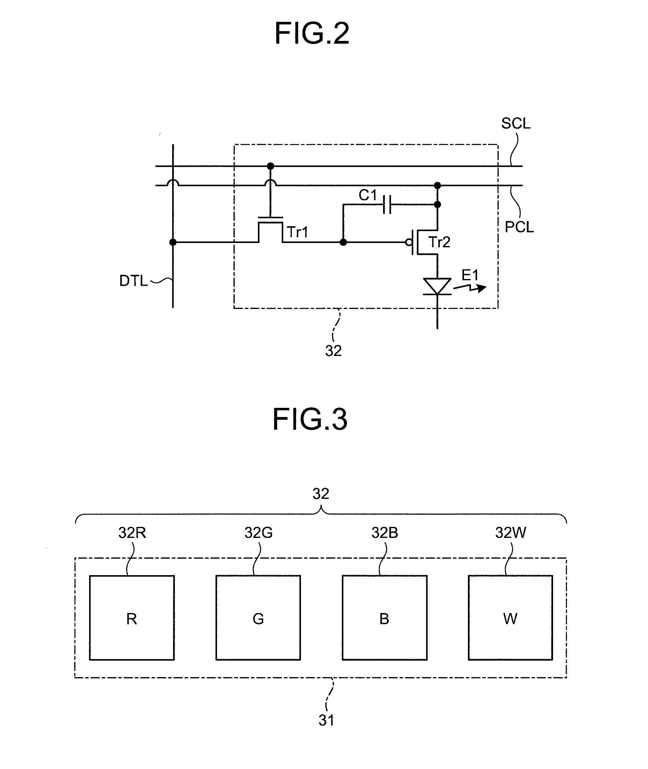
[0055]FIG. 1 is a schematic block diagram illustrating a configuration of the display device according to an embodiment. FIG. 2 is an exemplary diagram of a lighting drive circuit of a pixel including sub-pixels of an image display portion according to the embodiment. FIG. 3 is an exemplary diagram of arrangement of sub-pixels of the image display portion according to the embodiment. FIG. 4 is a cross-sectional view of the image display portion according to the embodiment.

[0056]As illustrated in FIG. 1, a display device 100 includes an image processing unit 70, an image display portion (image display panel) 30, an image display panel driving circuit 40 (hereinafter, referred to a driving circuit 40 as well) for controlling a drive of the image display panel 30. The image processing unit 70 includes a conversion unit 10 and a signal processing unit 20. The conversion unit 10 and the sign...

modification 1

[Modification 1]

[0100]Now, a modification 1 of the first embodiment is described below. The modification 1 is different from the first embodiment in that luminance attenuation ratio is calculated according to saturation. FIG. 10A is schematic diagram illustrating a relationship between saturation and luminance according to modification 1. FIG. 10B is schematic diagram illustrating a relationship between saturation and luminance attenuation ratio according to modification 1. FIG. 11A is a color pattern image prior to image processing method according to the embodiment. FIG. 11B is a color pattern image subsequent to image processing according to the first embodiment. FIG. 11C is a color pattern image subsequent to image processing method according to the modification 1.

[0101]In FIG. 10A, a vertical axis stands for luminance and a horizontal axis stands for saturation. In FIG. 10A, a line ‘c’ indicates a relationship between saturation and luminance under hue B. Here, hue B is not lim...

second embodiment

[0107]Now, second embodiment is described in detail below. FIG. 13 is schematic diagram illustrating a relationship between saturation and luminance attenuation ratio with various hues. FIG. 14 is a flowchart illustrating an image processing method according to a second embodiment. The second embodiment is different from the first embodiment in that a relationship between saturation and luminance attenuation ratio are stored associated with hue and luminance attenuation ratio is obtained on the basis of the identified hue and saturation. Elements substantially identical in function and configuration as those of the first embodiment are denoted by like reference numerals, and points where the modification differs from the first embodiment are mainly described below.

[0108]As described above, generally, the smaller saturation is, the higher luminance is because of coming close to a white. The greater saturation is, the lower luminance is. Furthermore, luminance varies in accordance wit...


PUM


Abstract

An image processing device comprising: a conversion unit to receive a first input signal including first color information, a first color being reproduced at pixels on the basis of the first color information, the first input signal including first color information obtained from an input image signal corresponding to a red component, a green component and a blue component, to specify saturation of the first color, and configured to obtain luminance attenuation ratio on the basis of a relationship previously stored between saturation and luminance attenuation ratio, and the saturation of the first color, and to output a second input signal including second color information whose luminance is decreased from the first color information on the basis of the luminance attenuation ratio corresponding to the first color information; and a signal processing unit configured to output an output signal for driving the pixels on the basis of the second input signal.

Description

CROSS-REFERENCE TO RELATED APPLICATIONS[0001]The present application claims priority to and incorporates by reference the entire contents of Japanese Patent Application No. 2013-219699 filed in Japan on Oct. 22, 2013, and Japanese Patent Application No. 2014-213105 filed in Japan on Oct. 17, 2014.BACKGROUND OF THE INVENTION[0002]1. Field of the Invention[0003]The present invention relates to an image processing device, a display device, an electronic device and a method for processing an image.[0004]2. Description of the Related Art[0005]Conventionally, the display device provided with an image display panel lighting the self-emitting elements like Organic Light Emitting Diode (OLED) needs no back light. Amount of power depends on the number of the self-emitting element in each of pixels. Therefore, it is effective for saving power consumption to reduce lighting of the self-emitting element by decreasing luminance of the self-emitting element. For example, Japanese patent laying ope...

Claims


Application Information

Patent Timeline
Patent Type & Authority Applications(United States)
IPC IPC(8): G09G3/20G09G3/32
CPCG09G3/2003G09G3/3208G09G2320/0666G09G2340/06G09G2320/0242G09G2330/023G09G2320/0233G09G3/3225G09G2300/0452G09G2320/0626G09G2330/021G09G2360/16
Inventor YATA, TATSUYANAKANISHI, TAKAYUKI
Owner JAPAN DISPLAY INC
Why Eureka
Try Eureka