Power semiconductor module

a technology of power semiconductor elements and semiconductor modules, applied in the field of power semiconductor modules, can solve problems such as deterioration of power semiconductor elements, and achieve the effect of efficient dissipation of heat generated by power semiconductor elements and simple configuration

Active Publication Date: 2015-04-30
MITSUBISHI ELECTRIC CORP
View PDF3 Cites 11 Cited by
  • Summary
  • Abstract
  • Description
  • Claims
  • Application Information

AI Technical Summary

Benefits of technology

[0017]A power semiconductor module according to the present invention is a power semiconductor module of insulation type, which contains a plurality of power semiconductor elements therein, the power semiconductor module includes a base plate as a metallic heat dissipating body, a first insulating layer provided on the base plate, and a first wiring pattern provided on the first insulating layer. And a predetermined region on the first wiring pattern is a pattern laminated region in which a second wiring pattern for a second layer is laminated via only a second insulating layer made of resin. Therefore, wirings in the power semiconductor module can be laminated in the pattern laminated region, whereby size reduction and inductance reduction in the power semiconductor module can be realized with a simple configuration. In addition, a power semiconductor element can be placed in a region other than the pattern laminated region on the first wiring pattern, whereby heat generated by the power semiconductor element can be efficiently dissipated.

Problems solved by technology

If the wiring inductance L is great, surge voltage that exceeds withstand voltage of the power semiconductor element occurs, which may cause deterioration in the power semiconductor element.

Method used


Image

  • Power semiconductor module
  • Power semiconductor module
  • Power semiconductor module

Examples


embodiment 1

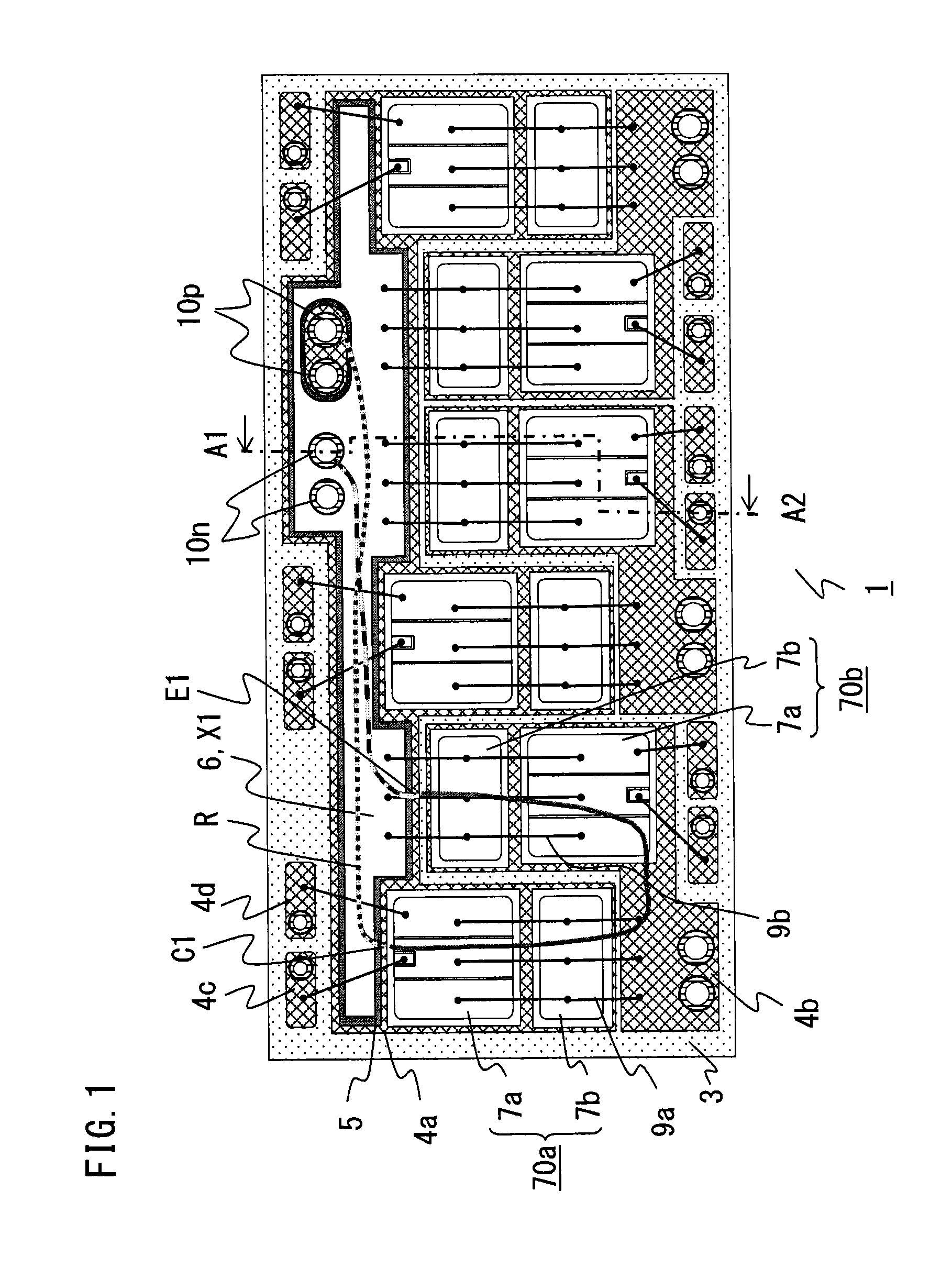
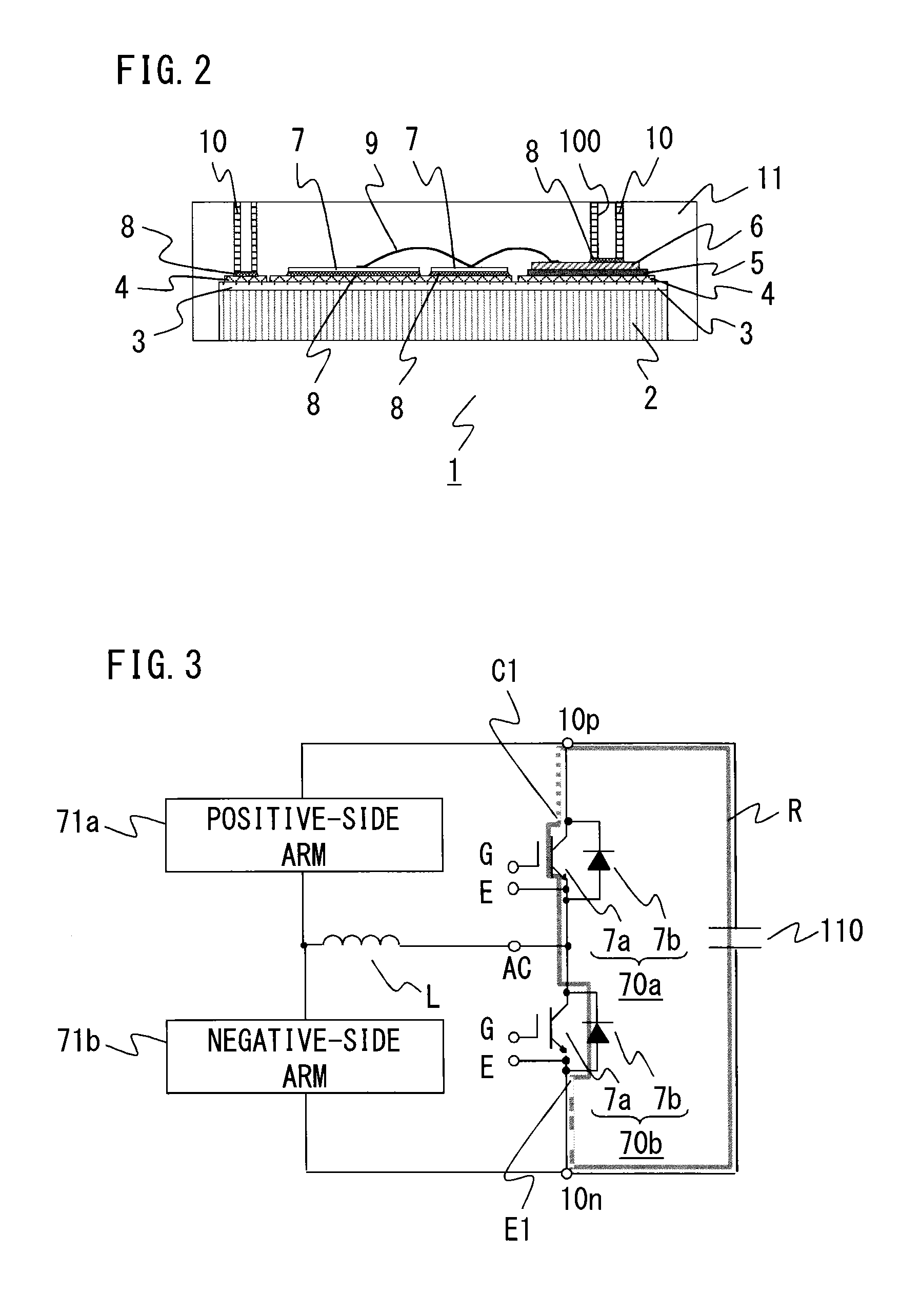
[0027]FIG. 1 is a plan view schematically showing the configuration of a power semiconductor module 1 in embodiment 1 of the present invention. FIG. 2 is an A1-A2 sectional view of the plan view in FIG. 1. The present embodiment 1 adopts a power semiconductor module having a so-called 6-in-1 structure and applicable to three-phase AC, as an example. The power semiconductor module with a 6-in-1 structure includes circuits for three phases in each of which two pairs of a self-arc-extinguishing type semiconductor element and a circulation diode connected in antiparallel are connected in series.

[0028]First, with reference to FIG. 1 and FIG. 2, the configuration of the power semiconductor module 1 will be briefly described. For making it easy to grasp the internal configuration of the power semiconductor module 1, a transfer mold resin is not shown in the plan view in FIG. 1.

[0029]The power semiconductor module 1 is a power semiconductor module of insulation type containing a plurality o...

embodiment 2

[0076]FIG. 4 is a plan view schematically showing the configuration of a power semiconductor module 1A in embodiment 2 of the present invention. FIG. 5 is a B1-B2 sectional view of the plan view in FIG. 4. For making it easy to grasp the internal configuration of the power semiconductor module 1A, the transfer mold resin 11 is not shown in the plan view in FIG. 4.

[0077]Also in the present embodiment 2, as in the above embodiment 1, a power semiconductor module having a 6-in-1 structure is adopted, and the power semiconductor module includes circuits for three phases in each of which two pairs of the self-arc-extinguishing type semiconductor element 7a and the circulation diode 7b connected in antiparallel are connected in series. A basic configuration such as placement of the power semiconductor elements 7a and 7b is almost the same as in the above embodiment 1, but the locations where a pattern of wiring for the gate electrode and a pattern of wiring for control of the emitter elec...

embodiment 3

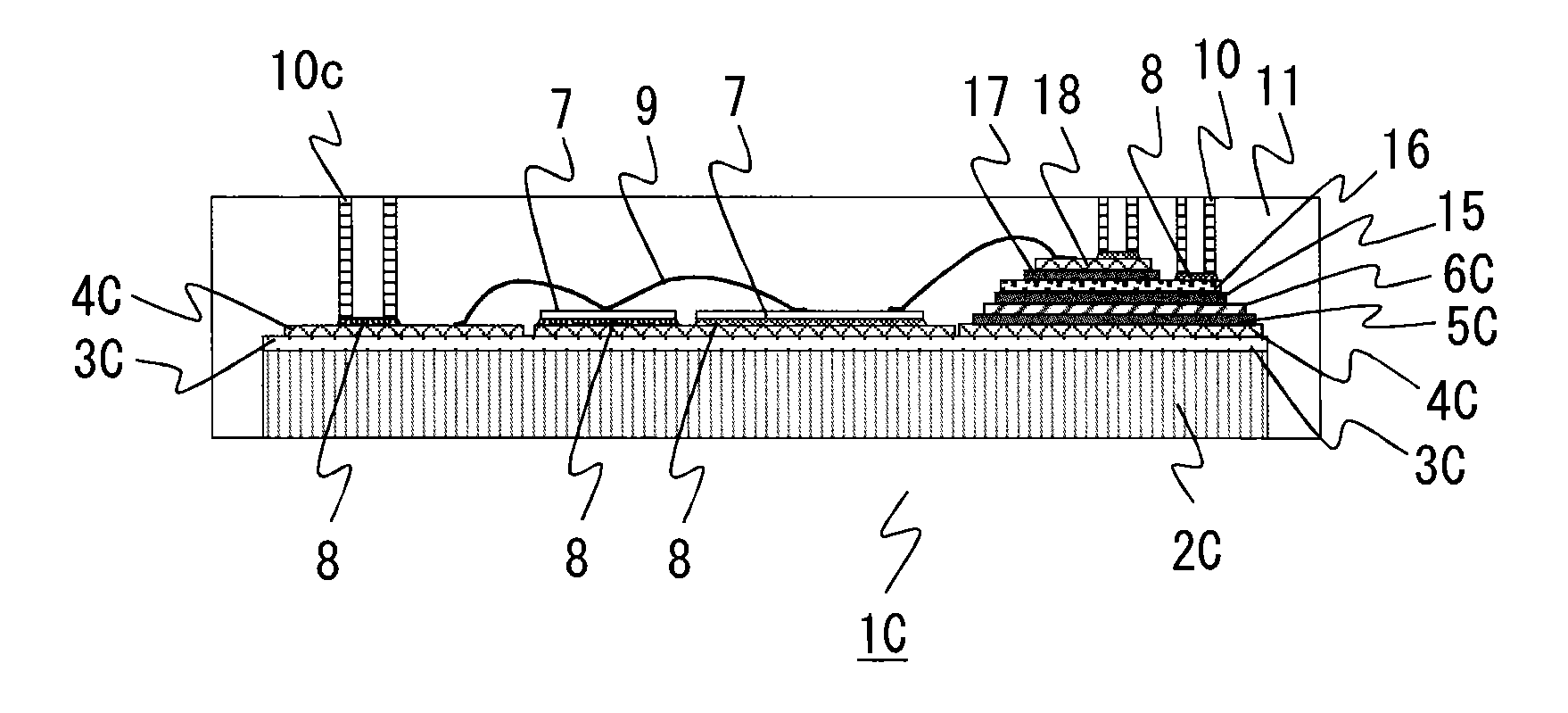
[0084]FIG. 6 is a plan view schematically showing the configuration of a power semiconductor module 1B in embodiment 3 of the present invention. FIG. 7 is a C1-C2 sectional view of the plan view in FIG. 6. The present embodiment 3 adopts a power semiconductor module having a so-called 2-in-1 structure, as an example.

[0085]The power semiconductor module 1B of the present embodiment 3 is composed of a circuit in which two pairs of the self-arc-extinguishing type semiconductor element 7a as the power semiconductor element 7 and the circulation diode 7b as the power semiconductor element 7 that are connected in antiparallel are connected in parallel to form one unit, and then two such units are connected in series.

[0086]Unlike the above embodiment 1 or embodiment 2, the power semiconductor module 1B of the present embodiment 3 is not a power semiconductor module of transfer-mold type which is sealed with a transfer mold resin. The power semiconductor module 1B of the present embodiment ...


PUM


Abstract

A power semiconductor module includes a base plate as a metallic heat dissipating body, a first insulating layer on the base plate, and a first wiring pattern on the first insulating layer. On a predetermined region that is a part of the first wiring pattern, a second wiring pattern for a second layer is laminated via only a second insulating layer made of resin, thereby forming a pattern laminated region. A power semiconductor element is mounted in a region other than the pattern laminated region on the first wiring pattern. The base plate, the first insulating layer, the first wiring pattern, the second insulating layer, the second wiring pattern, and the power semiconductor element are integrally sealed with a transfer mold resin, thus obtaining the power semiconductor module.

Description

TECHNICAL FIELD[0001]The present invention relates to a power semiconductor module of insulation type, used in a power conversion device such as an inverter.BACKGROUND ART[0002]Recently, size reduction of a power conversion device is required, so it is important to reduce the size of a power semiconductor module used therein.[0003]As a general structure of a power semiconductor module, a wiring pattern is formed via an insulating layer on a metal plate serving as a heat dissipating plate, a power semiconductor element is provided thereon and connected with each terminal by a wire bond, and then these are sealed with resin.[0004]Such power semiconductor modules can be roughly classified into two types, i.e., a case-type module which is sealed with silicone gel and a transfer-mold-type module which is sealed with epoxy resin (for example, see Patent Document 1 for the former one and Patent Document 2 for the latter one). The former case-type module often uses a ceramic insulating laye...

Claims


Application Information

Patent Timeline
Patent Type & Authority Applications(United States)
IPC IPC(8): H01L25/07H01L23/14H01L23/373H01L23/00H01L23/15H01L23/367
CPCH01L25/072H01L23/15H01L23/3675H01L23/3736H01L24/49H01L23/145H01L2224/48091H01L2924/13091H01L2924/10254H01L2924/10272H01L2924/1033H01L2224/4911H01L2924/13055H01L23/049H01L23/24H01L23/3735H01L23/4334H01L23/49811H01L23/3107H01L24/29H01L24/32H01L24/45H01L24/48H01L24/73H01L2224/291H01L2224/32225H01L2224/45124H01L2224/45147H01L2224/48137H01L2224/48139H01L2224/48227H01L2224/49175H01L2224/73265H01L2924/1203H05K1/053H05K3/284H05K2203/1316H01L2924/30107H01L2924/3011H01L2924/1305H01L25/18H01L2224/04042H01L2924/10253H01L2924/1815H01L2224/45015H01L2924/15787H01L2924/181H01L2224/0603H01L2224/49111H01L2224/49113H01L2924/00012H01L2924/014H01L2924/00H01L2924/00014H05K1/05
Inventor TAMADA, YOSHIKOOKA, SEIJI
Owner MITSUBISHI ELECTRIC CORP
Why Eureka
Try Eureka