This helps you quickly interpret patents by identifying the three key elements:
Problems solved by technology
Method used
Benefits of technology
Benefits of technology
The present invention provides a semiconductor module for electric power that can be smaller and have less wiring inductance.
Problems solved by technology
If this inductance value becomes large, accompanying electric voltage heightening of the electric source electric voltage, electric current enlarging and speed heightening of the device, then it becomes a bad influence on the device.
Specifically, a through electric current becomes a problem at the ON time and a jumping electric voltage at the OFF time, which, in the worst case, leads to destruction of an element.
Method used
Image
Click on the blue label to locate the original text in one second.
Reading with bidirectional positioning of images and text.
Examples
embodiment 1
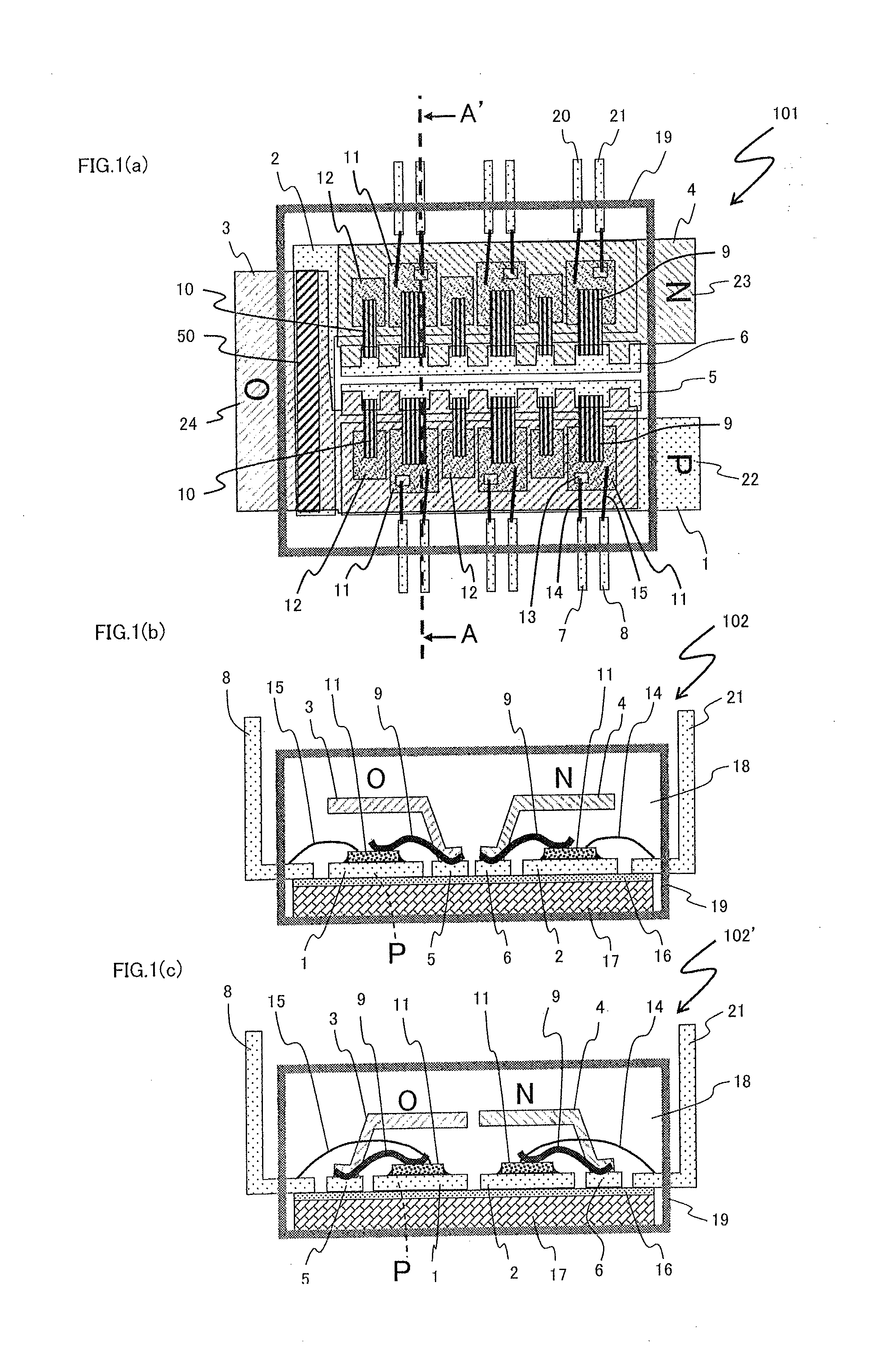
[0104]Shown in FIG. 1(a) is the module configuration 101 which is a plan view of the semiconductor module for electric power of a resin-sealing-type of Embodiment 1 of the present invention.
[0105]Moreover, shown in FIG. 1(b) is the section configuration 102 of the semiconductor module for electric power of the present Embodiment 1 such that cutting is carried out with A-A′ in FIG. 1(a).
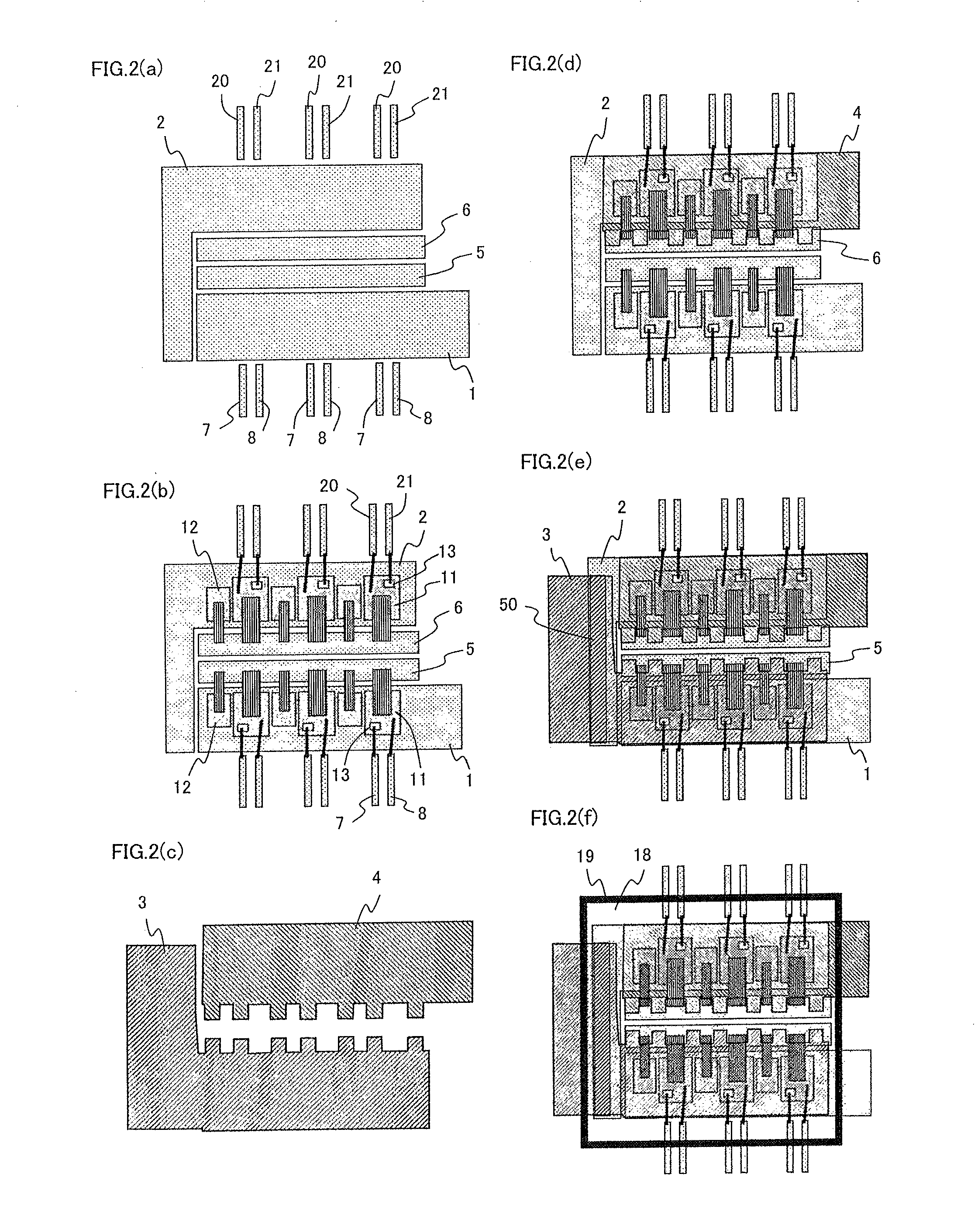
[0106]Moreover, in FIG. 2(a)-FIG. 2(f), an assembly flow diagram of the semiconductor module for electric power of the present Embodiment 1 is shown. FIG. 2(a)-FIG. 2(f) show, respectively, plan views at the time of assembly of the semiconductor module for electric power of the present Embodiment 1.
[0107]Before descriptions are given regarding the configuration of the semiconductor module for electric power of the present Embodiment 1, for a start descriptions are given regarding the assembly process of the semiconductor module for electric power of the present Embodiment 1, using FIG. 2(a)-FIG. 2(f)....
embodiment 2
[0147]In Embodiment 1, the present invention has been described with a module of a resin-sealing-type, but the concept of the present invention is not limited to this and, even if applied to a module formed on a metal insulating substrate, similar effects are obtained. Even with other embodiments, similar effects are obtained.
[0148]As Embodiment 2 of the present invention, the module configuration 103 which is a plan view of the semiconductor module for electric power of a metal-insulating-substrate-type is shown in FIG. 3(a).
[0149]Moreover, shown in FIG. 3(b) is the section configuration 104 of the semiconductor module for electric power of the present Embodiment 2 such that cutting is carried out with B-B′ in FIG. 3(a).
[0150]Moreover, in FIG. 4(a)-FIG. 4(f), an assembly flow diagram of the semiconductor module for electric power of the present Embodiment 2 is shown. FIG. 4(a)-FIG. 4(f) show, respectively, plan views at the time of assembly of the semiconductor module for electric ...
embodiment 3
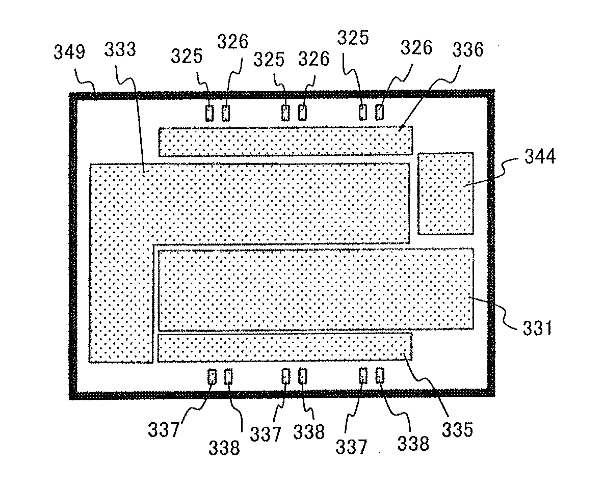
[0198]Shown in FIG. 5(a) is the module configuration 1101 which is a plan view of the semiconductor module for electric power of a resin-sealing-type of Embodiment 3 of the present invention.
[0199]Moreover, shown in FIG. 5(b) is the section configuration 1102 of the semiconductor module for electric power of the present Embodiment 3 such that cutting is carried out with A-A′ in FIG. 5(a).
[0200]Moreover, in FIG. 6(a)-FIG. 6(e), an assembly flow diagram of the semiconductor module for electric power of the present Embodiment 3 is shown. FIG. 6(a)-FIG. 6(e) show, respectively, plan views at the time of assembly of the semiconductor module for electric power of the present Embodiment 3.
[0201]Before descriptions are given regarding the configuration of the semiconductor module for electric power of the present Embodiment 3, for a start descriptions are given regarding the assembly process of the semiconductor module for electric power of the present Embodiment 3, using FIG. 6(a)-FIG. 6(e...
PUM
Abstract
Included are: the third frame which is electrically connected to the first intermediate frame and is arranged above the first frame; the fourth frame which is electrically connected to the second intermediate frame and is arranged above the second frame; the electric source terminal part which is provided on an extension of the first frame; the ground terminal part which is provided on an extension of the fourth frame; and the output terminal part which is provided on an extension to which the second frame and the third frame are electrically joined, wherein the third frame and the fourth frame are arranged in parallel with each other, and the electric source terminal part, the ground terminal part and the output terminal part are arranged in a manner such that induced electric voltages, which are generated in the third frame and the fourth frame, become in reverse directions with each other.
Description
CROSS-REFERENCE TO RELATED APPLICATIONS[0001]This application is a U.S. national phase application of PCT International Patent Application No. PCT / JP2013 / 002941 filed May 7, 2013, claiming the benefit of priority of Japanese Patent Application No. 2012-112453 filed May 16, 2012 and Japanese Patent Application No. 2012-130680 filed Jun. 8, 2012, all of which are incorporated by reference herein in their entirety.TECHNICAL FIELD[0002]An aspect of the present invention is what relates to structure of a semiconductor module for electric power.BACKGROUND ART[0003]Of a semiconductor module for electric power which converts electric power, high efficiency is required from the viewpoint of energy saving.[0004]Because of that, as for a semiconductor element, progressing is a transition from an insulating gate-type bipolar transistor (IGBT) to a transistor, using a wide-band-gap-system semiconductor element (SiC or GaN) for electric power. Particularly, an insulating gate-type transistor usin...
Claims
Application Information
Patent Timeline
Application Date:The date an application was filed.
Publication Date:The date a patent or application was officially published.
First Publication Date:The earliest publication date of a patent with the same application number.
Issue Date:Publication date of the patent grant document.
PCT Entry Date:The Entry date of PCT National Phase.
Estimated Expiry Date:The statutory expiry date of a patent right according to the Patent Law, and it is the longest term of protection that the patent right can achieve without the termination of the patent right due to other reasons(Term extension factor has been taken into account ).
Invalid Date:Actual expiry date is based on effective date or publication date of legal transaction data of invalid patent.

