Multilayer ceramic electronic component and mother ceramic multilayer body

a multi-layer ceramic and electronic component technology, applied in the direction of fixed capacitors, stacked capacitors, fixed capacitor details, etc., can solve the problems of small inner electrode density, easy generation of delamination between, and difficulty in pressing pressure to act on the lead-out region. to achieve the effect of preventing delamination

Inactive Publication Date: 2015-04-30
MURATA MFG CO LTD
View PDF8 Cites 5 Cited by
  • Summary
  • Abstract
  • Description
  • Claims
  • Application Information

AI Technical Summary

Benefits of technology

This patent aims to provide a multilayer ceramic electronic component and a mother ceramic multilayer body that are resistant to delamination between an inner electrode and a ceramic layer. The technical effects of this patent text are that it reduces the likelihood of reliability issues in the electronic component caused by delamination between the inner electrode and ceramic layer.

Problems solved by technology

When the difference in the density of the inner electrodes between the opposing region and the lead-out region is larger, it is difficult for a pressing pressure to act on the lead-out region on which the density of the inner electrodes is small.
This results in delamination being easily generated between the inner electrodes and the ceramic layers.
This problem is significant when individual ceramic multilayer bodies are manufactured by cutting a raw mother ceramic multilayer body.
However, even the isostatic pressing as described in Japanese Unexamined Patent Application Publication No. 2-161713 does not sufficiently suppress the delamination that occurs when the raw mother ceramic multilayer body is cut in the ceramic electronic component in which the number of inner electrodes that are laminated is increased.

Method used


Image

  • Multilayer ceramic electronic component and mother ceramic multilayer body
  • Multilayer ceramic electronic component and mother ceramic multilayer body
  • Multilayer ceramic electronic component and mother ceramic multilayer body

Examples


Embodiment Construction

[0027]Hereinafter, various preferred embodiments of the present invention will be explained with reference to the drawings.

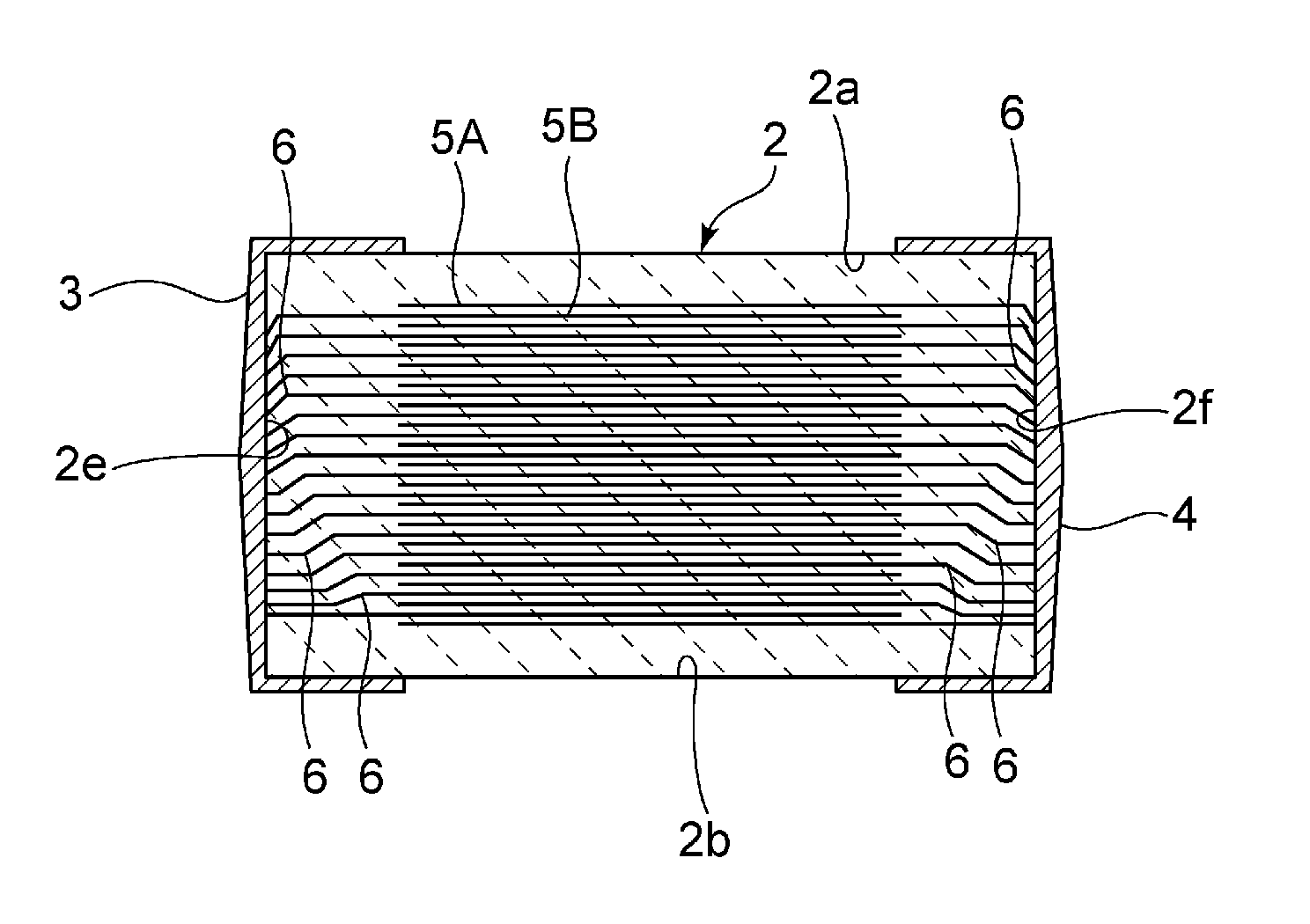
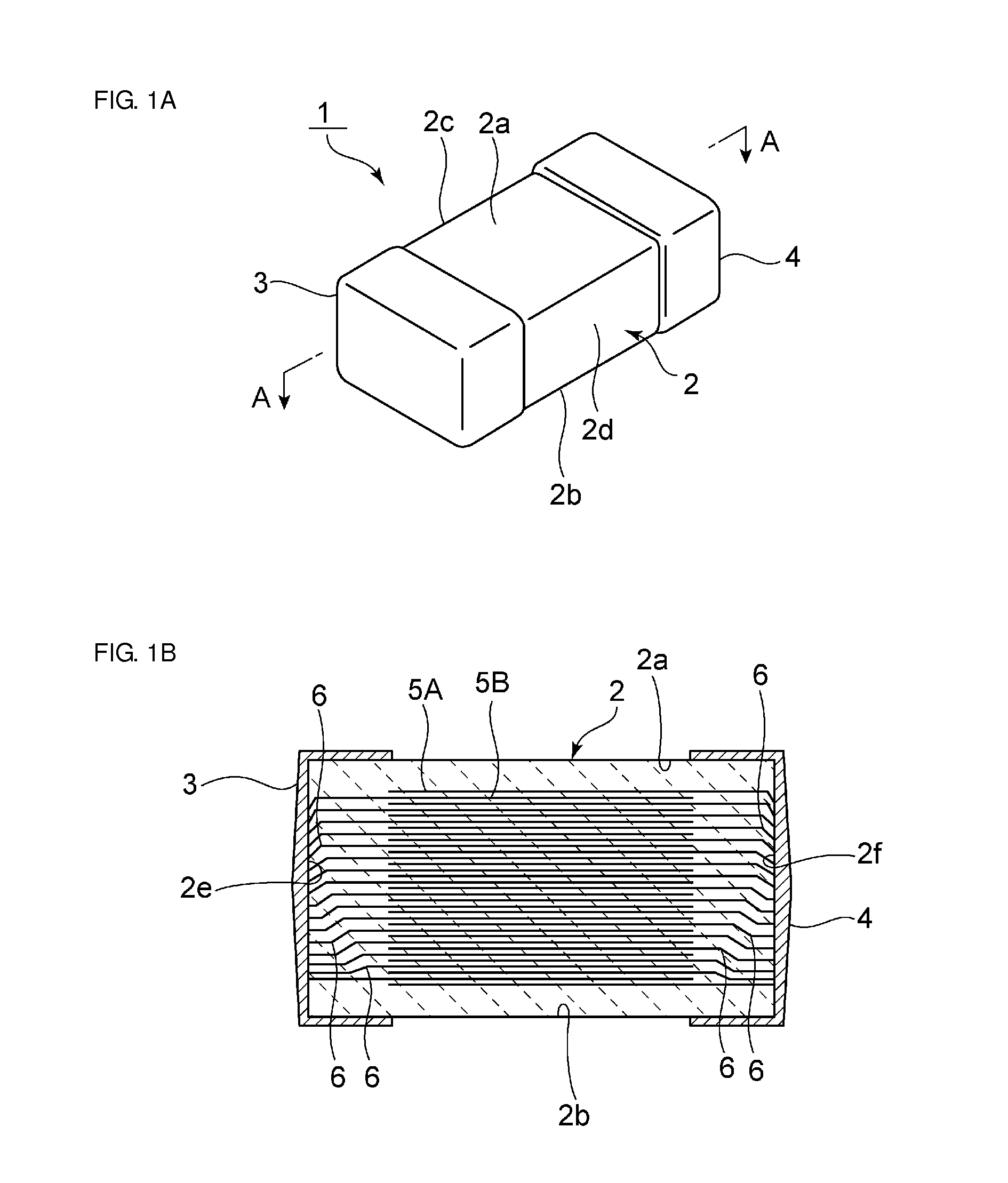
[0028]FIG. 1A is a perspective view illustrating a multilayer ceramic capacitor according to a preferred embodiment of the present invention and FIG. 1B is a cross-sectional view cut along a line A-A in FIG. 1A.

[0029]A multilayer ceramic capacitor 1 includes a ceramic body 2, first and second outer electrodes 3 and 4, and inner electrodes 5A and 5B. The ceramic body 2 includes a plurality of ceramic layers laminated on each other. The ceramic body 2 preferably has a rectangular or substantially rectangular parallelepiped shape including first and second main surfaces 2a and 2b, first and second side surfaces 2c and 2d, and first and second end surfaces 2e and 2f. The first and second main surfaces 2a and 2b extend along the lengthwise direction and the width direction. The first and second side surfaces 2c and 2d extend along the lengthwise direction and the thi...


PUM

PropertyMeasurementUnit
angleaaaaaaaaaa
angleaaaaaaaaaa
heightaaaaaaaaaa

Abstract

A multilayer ceramic electronic component includes a ceramic body, first and second outer electrodes, and a plurality of first and second inner electrodes opposing each other across ceramic layers in a lamination direction of the ceramic body. At least two inner electrodes among the plurality of first and second inner electrodes include bent portions on lead-out regions as portions on which the plurality of first inner electrodes and the plurality of second inner electrodes do not oppose each other across the ceramic layers in the lamination direction, and vertexes of the bent portions of the inner electrodes adjacent in the lamination direction are at different positions in a lead-out direction.

Description

BACKGROUND OF THE INVENTION[0001]1. Field of the Invention[0002]The present invention relates to a multilayer ceramic electronic component and a mother ceramic multilayer body for manufacturing a multilayer ceramic electronic component.[0003]2. Description of the Related Art[0004]In recent years, in a multilayer ceramic electronic component such as a multilayer ceramic capacitor, size reduction and an increase in an electrostatic capacitance are desired. Therefore, the number of inner electrodes that are laminated is increased. As the number of inner electrodes that are laminated is increased, the inner electrodes are crowded in an opposing region where the inner electrodes that are connected to different potentials oppose each other in the lamination direction. Thus, the density of the inner electrodes becomes higher in the opposing region.[0005]In a lead-out region where the inner electrodes do not oppose each other, the inner electrodes that are led out are any one of the inner e...

Claims


Application Information

Patent Timeline
Patent Type & Authority Applications(United States)
IPC IPC(8): H01G4/30H01G4/38H01G4/248H01G4/012H01G4/12
CPCH01G4/30H01G4/012H01G4/38H01G4/248H01G4/12H01G4/232
Inventor SAKAI, SATOKI
Owner MURATA MFG CO LTD
Why Eureka
Try Eureka