System and Method for a Millimeter Wave Circuit Board

a millimeter wave and circuit board technology, applied in the field of circuit boards, can solve the problems of high frequency circuit adaptation, attenuation and mismatch of high frequency rf signals, and additional problems with thermal managemen

Active Publication Date: 2015-04-30
INFINEON TECH AG
View PDF6 Cites 9 Cited by
  • Summary
  • Abstract
  • Description
  • Claims
  • Application Information

AI Technical Summary

Problems solved by technology

As the operating frequencies of RF systems continue to increase, however, the generation of signals at such high frequencies poses a number of major challenges.
One such challenge in the interfacing of millimeter wave signals to and from integrated circuits.
At high frequencies, bond wires, package contacts, printed circuit board (PCB) traces, board capacitance, and other parasitics may potentially cause attenuation and mismatch of high frequency RF signals.
In higher power millimeter wave systems, additional issues may arise with respect to thermal management.
These conductive layers and thermal dissipation structures may increase parasitic capacitances and inductances that may degrade RF performance.

Method used


Image

  • System and Method for a Millimeter Wave Circuit Board
  • System and Method for a Millimeter Wave Circuit Board
  • System and Method for a Millimeter Wave Circuit Board

Examples


Embodiment Construction

[0017]The making and using of various embodiments are discussed in detail below. It should be appreciated, however, that the various embodiments described herein are applicable in a wide variety of specific contexts. The specific embodiments discussed are merely illustrative of specific ways to make and use various embodiments, and should not be construed in a limited scope.

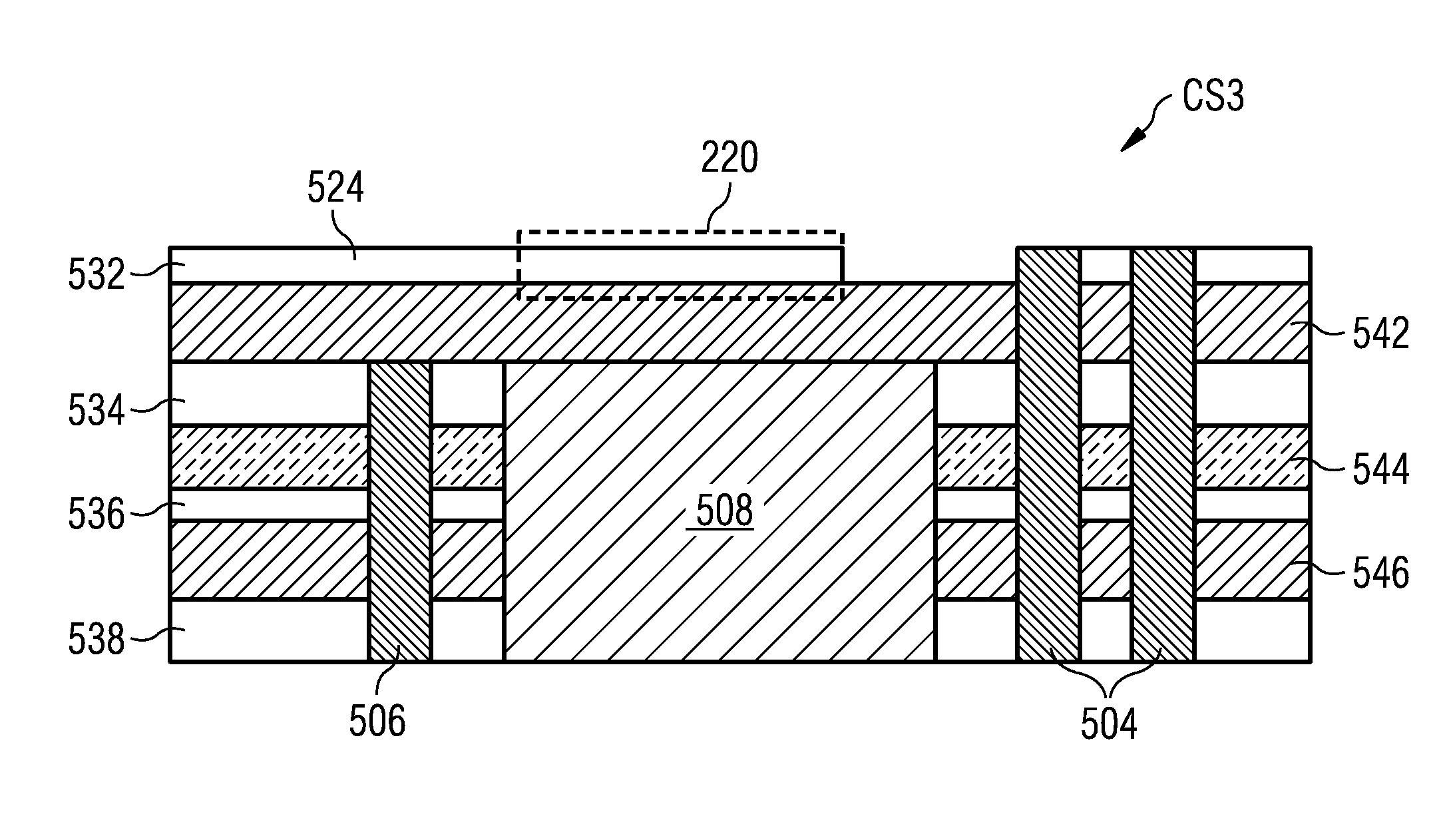
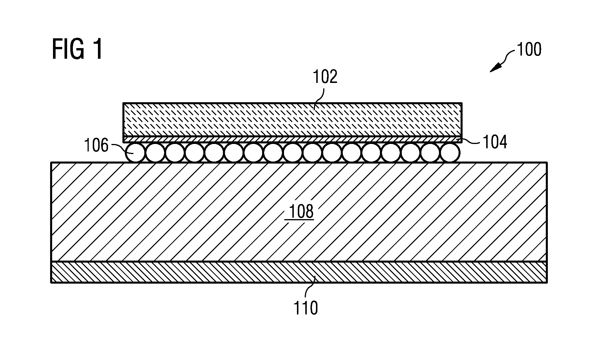
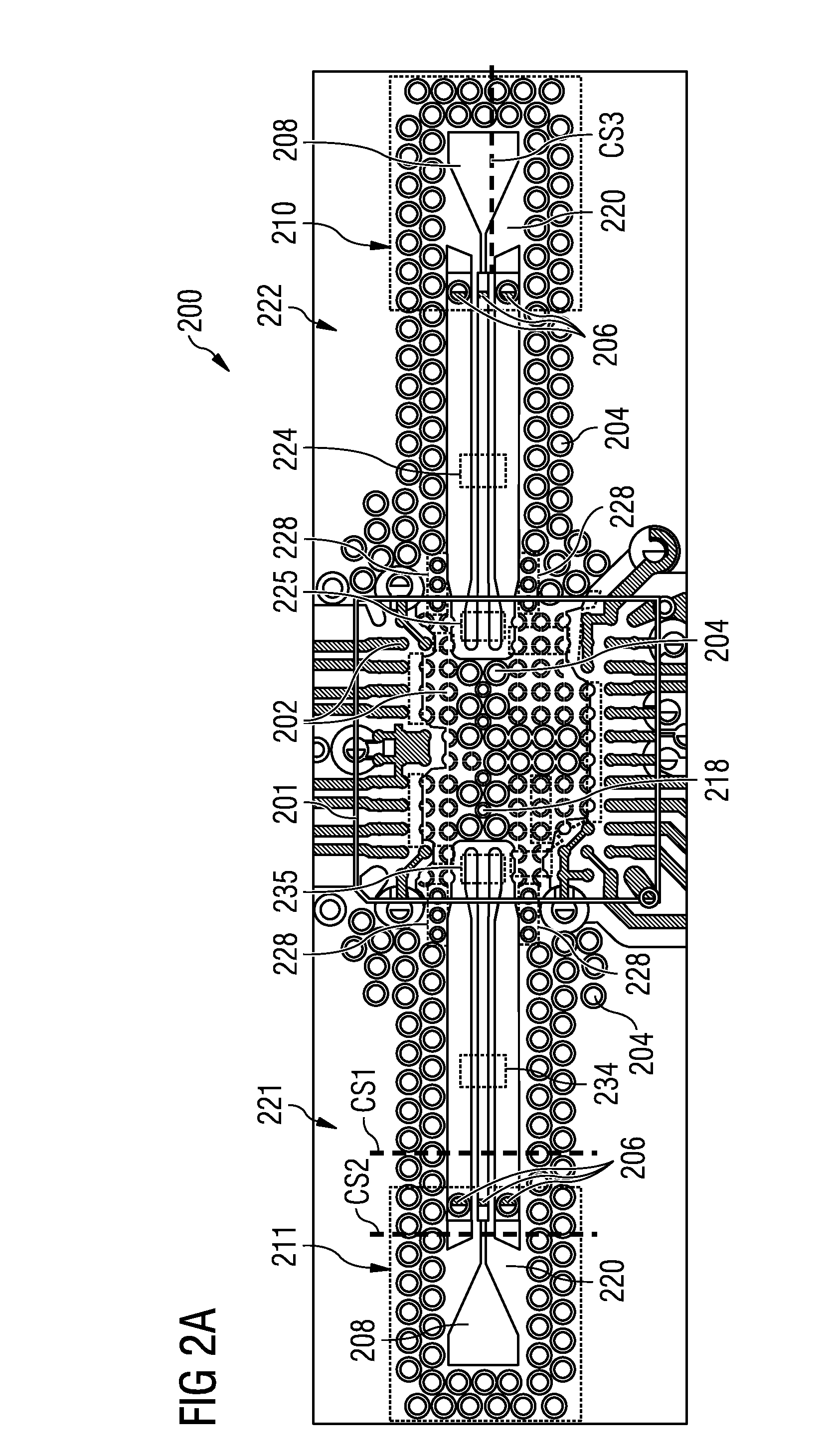
[0018]Description is made with respect to various embodiments in a specific context, namely embedded system, and more particularly, to a millimeter wave circuit board. Some of the various embodiments described herein include radio frequency (RF) transceivers, circuit boards, printed circuit boards (PCB), PCBs with embedded antennas, thermal management on a PCB and bonded IC, waveguides, waveguide shielding, and others. Many embodiments herein are described with signals having frequencies in the RF range and particular applications may focus on radio signals with millimeter (mm) wavelength signals, which generally...


PUM


Abstract

According to an embodiment, a circuit board includes a signal line including at least portion of a first conductive layer that has a first portion extending over a cavity in the circuit board from a first side of the cavity. The circuit board also includes a first plurality of conductive vias surrounding the cavity and the first plurality of vias include at least one blind via disposed adjacent to the first side of the cavity.

Description

TECHNICAL FIELD[0001]The present invention relates generally to circuit boards, and, in particular embodiments, to a system and method for a millimeter wave circuit board.BACKGROUND[0002]Applications in the millimeter-wave frequency regime have gained significant interest in the past few years due to the rapid advancement in low cost semiconductor technologies such as silicon germanium (SiGe) and fine geometry complementary metal-oxide semiconductor (CMOS) processes. Availability of high speed bipolar and metal-oxide semiconductor (MOS) transistors has led to a growing demand for integrated circuits for mm-wave applications at 60 GHz, 77 GHz, and 80 GHz and also beyond 100 GHz. Such applications include, for example, automotive radar and multi-gigabit communication systems.[0003]As the operating frequencies of RF systems continue to increase, however, the generation of signals at such high frequencies poses a number of major challenges. One such challenge in the interfacing of milli...

Claims


Application Information

Patent Timeline
Patent Type & Authority Applications(United States)
IPC IPC(8): H01P3/12H04B10/2575H05K1/18H04B10/572H05K1/11H05K1/02
CPCH01P3/12H05K1/116H05K1/0242H04B10/2575H05K1/181H04B10/572H05K1/0206H01P5/107H05K1/024H05K1/0251H05K3/4697H01L23/13
Inventor TROTTA, SAVERIOBAL, JAGJIT SINGHWOJNOWSKI, MACIEJSELER, ERNSTPOUR MOUSAVI, MEHRAN
Owner INFINEON TECH AG
Why Eureka
Try Eureka