Imaging Array with Improved Dynamic Range Utilizing Parasitic Photodiodes

a technology of parasitic photodiodes and imaging arrays, which is applied in the direction of radio frequency controlled devices, instruments, transistors, etc., can solve the problems of increasing the cost of imaging arrays and artifacts in images

Active Publication Date: 2015-05-07
BAE SYST IMAGING SOLUTIONS
View PDF8 Cites 24 Cited by
  • Summary
  • Abstract
  • Description
  • Claims
  • Application Information

AI Technical Summary

Benefits of technology

[0005]The present invention includes a pixel sensor, a method for measuring a light exposure using that pixel sensor, and memory arrays constructed from that pixel sensor. A pixel sensor according to the present invention includes a photodiode, a floating diffusion node, and a readout amplifier. The photodiode is characterized by a first light conversion efficiency. A gate selectiv...

Problems solved by technology

In principle, the maximum well capacity can be increased by utilizing larger photodiodes; however, this solution increases the cost of the imaging array and requires processing electronics that can deal with the larg...

Method used


Image

  • Imaging Array with Improved Dynamic Range Utilizing Parasitic Photodiodes
  • Imaging Array with Improved Dynamic Range Utilizing Parasitic Photodiodes
  • Imaging Array with Improved Dynamic Range Utilizing Parasitic Photodiodes

Examples


Embodiment Construction

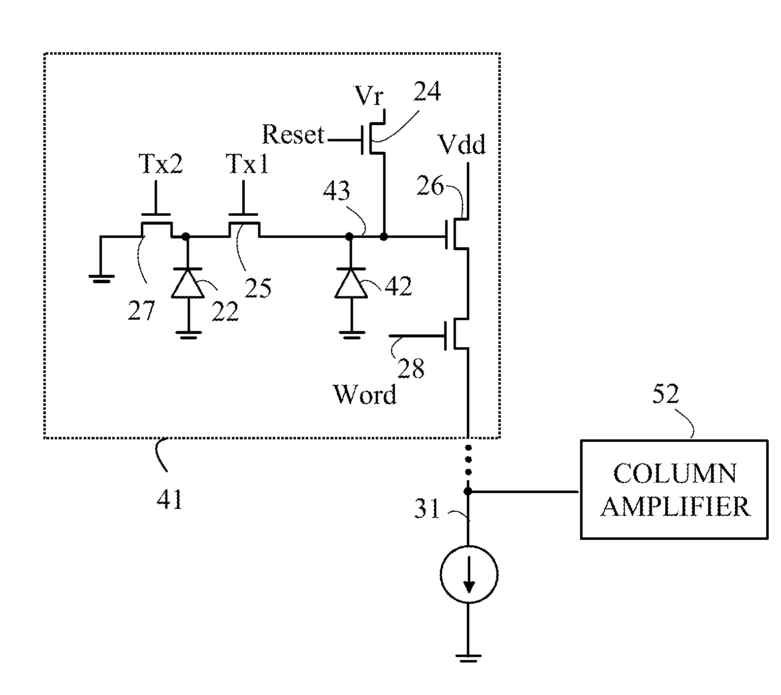
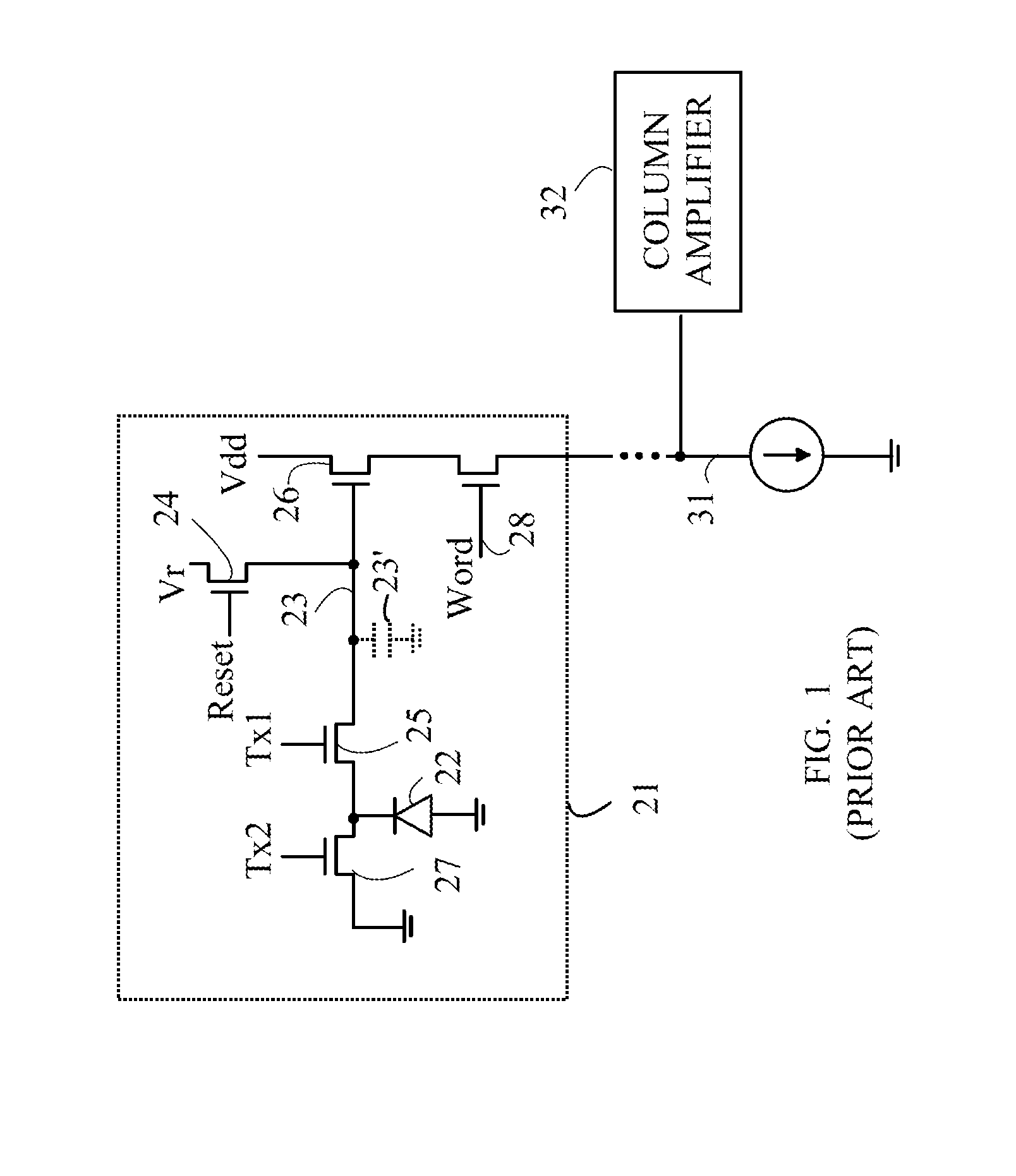
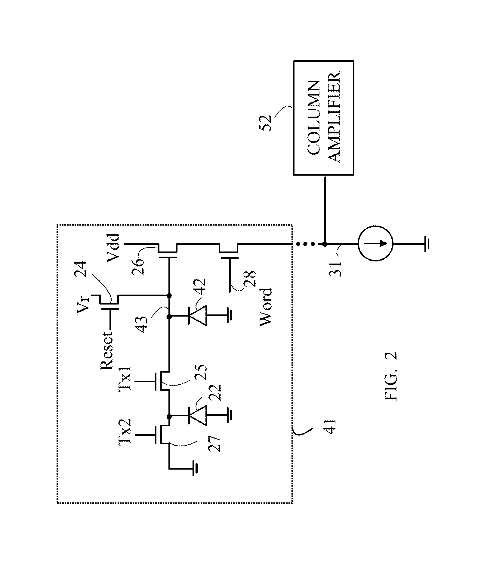
[0014]The manner in which the present invention provides its advantages can be more easily understood with reference to FIG. 1, which is a schematic drawing of a typical prior art pixel sensor in one column of pixel sensors in an imaging array. Pixel sensor 21 includes a photodiode 22 that measures the light intensity at a corresponding pixel in the image. Initially, photodiode 22 is reset by placing gate 25 in a conducting state and connecting floating diffusion node 23 to a reset voltage, Vr. Gate 25 is then closed and photodiode 22 is allowed to accumulate photoelectrons. A potential on gate 27 sets the maximum amount of charge that can be accumulated on photodiode 22. If more charge is accumulated than allowed by the potential on gate 27, the excess charge is shunted to ground through gate 27.

[0015]After photodiode 22 has been exposed, the charge accumulated in photodiode 22 is typically measured by noting the change in voltage on floating diffusion node 23 when the accumulated ...


PUM


Abstract

A pixel sensor having a main photodiode and a parasitic photodiode and a method for reading out that pixel sensor are disclosed. The parasitic photodiode also serves the function of a floating diffusion node in the pixel. The pixel sensor is read by first determining the exposure as measured by the parasitic photodiode and then determining the exposure as read by the main photodiode. One of the two exposure measurements is chosen as the pixel output. The main photodiode has a light conversation efficiency chosen such that one of the two measurements will provide a measurement of the exposure over a dynamic range that is greater than that of either the main photodiode or the parasitic photodiode utilized separately.

Description

RELATED APPLICATIONS[0001]This application is a continuation-in-part of U.S. patent application Ser. No. 13 / 936,974 filed on 8 Jul. 2013.BACKGROUND OF THE INVENTION[0002]CMOS imaging sensors are widely used in cameras and other imaging applications. The imaging sensors typically include a two-dimensional array of pixel sensors. Each pixel sensor includes a photodiode that measures the image intensity at a corresponding point in the image. The dynamic range of the image sensor is the ratio of the minimum amount of light that can be measured to the maximum amount. An image is formed by first emptying the photodiodes of any accumulated charge and then exposing the photodiodes to the image. Each photodiode accumulates charge at a rate determined by the light intensity emitted by the image at the corresponding point in the image, referred to as a pixel. In general, the amount of charge that can be accumulated in a photodiode has a maximum value, referred to as the maximum well capacity. ...

Claims


Application Information

Patent Timeline
IPC IPC(8): H01L27/146
CPCH01L27/14643H01L27/14609H01L27/14612H01L27/14656H04N25/585
Inventor FOWLER, BOYD
Owner BAE SYST IMAGING SOLUTIONS
Why Eureka
Try Eureka