

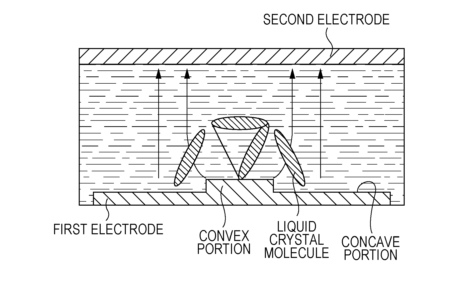
Liquid crystal display device
a liquid crystal display and display device technology, applied in non-linear optics, instruments, optics, etc., can solve the problems of deterioration of responsive characteristics to voltage and lowering transmittance, and achieve the effect of reliably suppressing problems, enhancing orientation regulating force, and reliably defining tilt states
- Summary
- Abstract
- Description
- Claims
- Application Information
AI Technical Summary
Benefits of technology
Problems solved by technology
Method used
Image

Examples
example 1
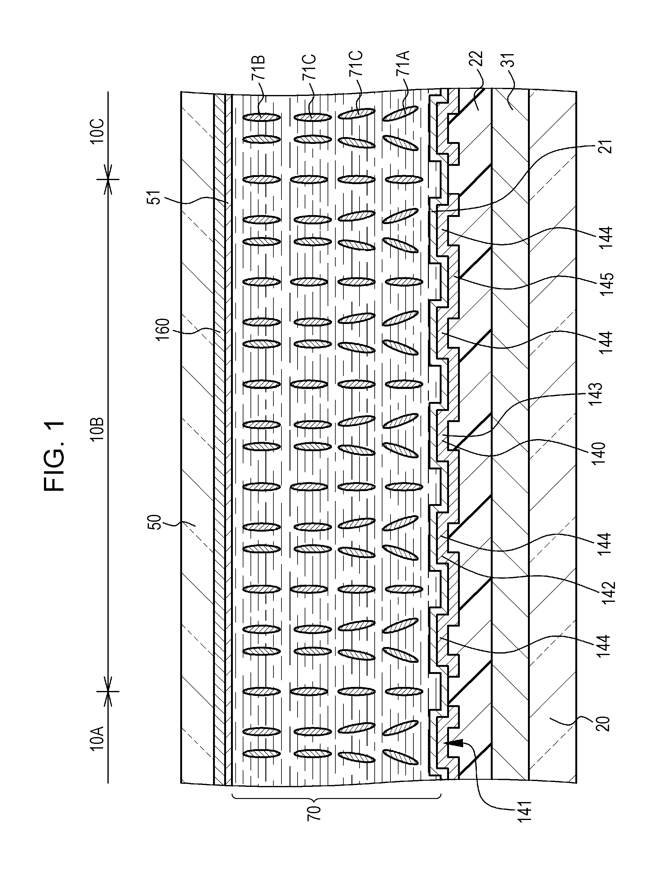
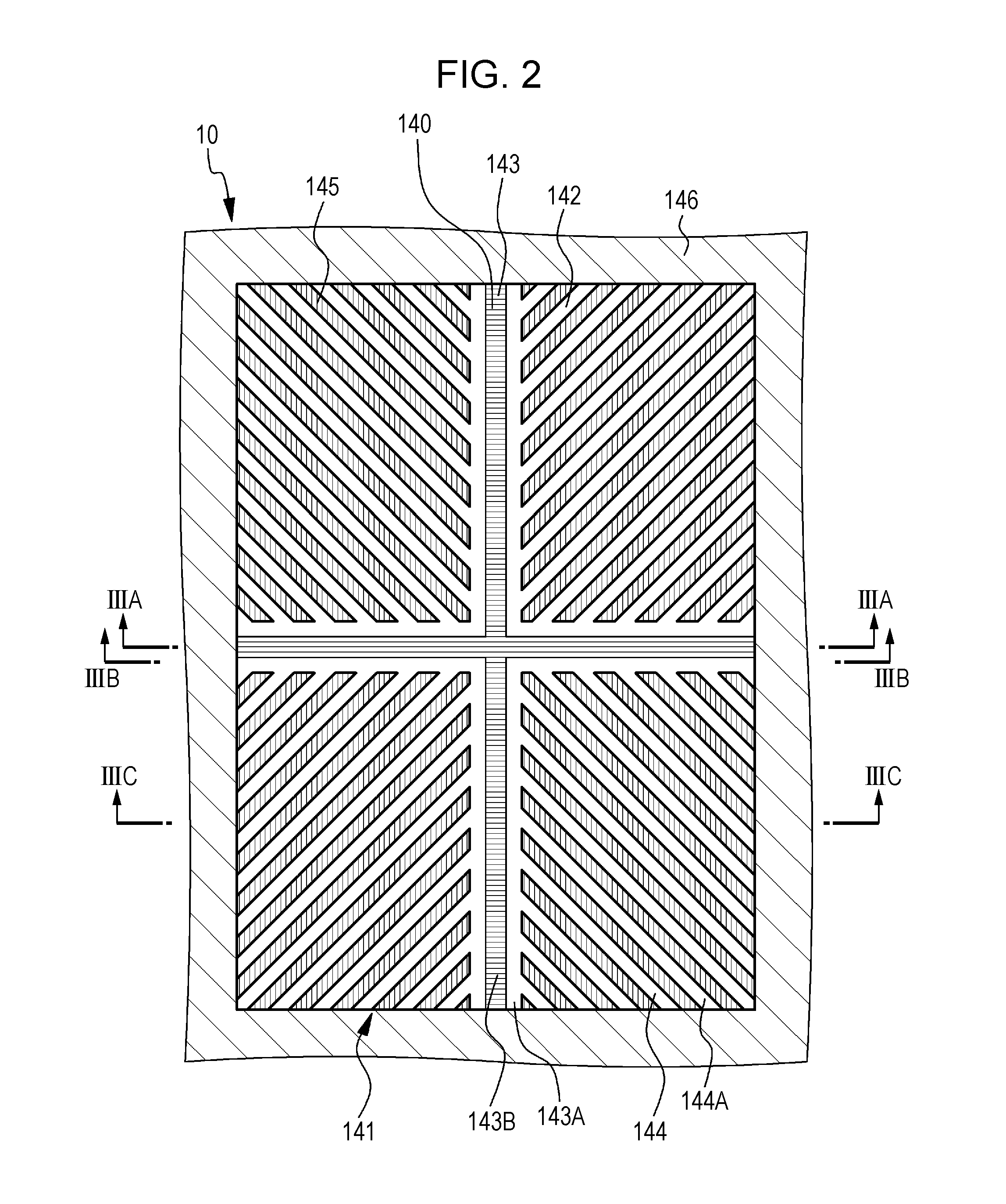
[0087]Example 1 relates to a liquid crystal display device according to Mode 1 of the present disclosure, and more specifically to a liquid crystal display device according to Mode 1-A of the present disclosure. FIG. 1 shows a partial end surface view schematically showing the liquid crystal display device according to Example 1. FIG. 2 is a planar view schematically showing the first electrode corresponding to a pixel configuring the liquid crystal display device according to Example 1. FIGS. 3A, 3B, and 3C are partial cross-sectional views schematically showing the first electrode and the like taken along the arrow IIIA-IIIA, the arrow IIIB-IIIB, and the arrow IIIC-IIIC in FIG. 2. FIG. 3D is a partial cross-sectional view schematically showing a part of FIG. 3C in an enlarged manner.
[0088]The liquid crystal display device according to Example 1 or Examples 2 to 9, which will be described later, is a liquid crystal display device in which a plurality of pixels 10 are aligned such t...
example 2
[0146]Example 2 is a modification of Example 1. FIG. 5 is a planar view schematically showing a first electrode corresponding to a pixel configuring a liquid crystal display device according to Example 2. FIGS. 7A and 7B are partial cross-sectional views schematically showing the first electrode and the like taken along the arrow VIIA-VIIA and the arrow VIIB-VIIB in FIG. 5.
[0147]In Example 2, a top surface of a convex stem portion 143 is configured by a top surface 143C at a center portion of the convex stem portion 143, a top surface 143B positioned on both sides of the top surface 143C, and a top surface 143A positioned outside the top surface 143B. Three stepped portions are present at the convex stem portion 143 as described above, and when a concave portion 145 is regarded as a reference, the top surface 143A, the top surface 143B, and the top surface 143C are higher in this order. In addition, a cross-sectional shape of the convex stem portion 143 when the convex stem portion ...
example 3
[0149]Example 3 is also a modification of Example 1. FIG. 6 is a planar view schematically showing a first electrode corresponding to a pixel configuring a liquid crystal display device according to Example 3. FIG. 7C is a partial end surface view schematically showing the first electrode and the like taken along the arrow XIIC-XIIC in FIG. 6, and FIG. 7D shows a partial end surface view schematically showing a part of FIG. 7C in an enlarged manner.
[0150]In Example 3, a cross-sectional shape of a branched convex portion 144 when the branched convex portion 144 is cut by a virtual vertical plane which is orthogonal to an extending direction of the branched convex portion 144 is a cross-sectional shape in which the stepped portion declines from the center of the cross-sectional shape of the branched convex portion 144 toward the edge of the cross-sectional shape of the branched convex portion 144. Specifically, a top surface of the branched convex portion 144 is configured by a top su...
PUM
| Property | Measurement | Unit |
|---|---|---|
| dielectric constant | aaaaa | aaaaa |
| widths | aaaaa | aaaaa |
| widths | aaaaa | aaaaa |
Abstract
Description
Claims
Application Information