

Cluster-batch type system for processing substrate
a technology of substrate and processing equipment, which is applied in the direction of pile separation, transportation and packaging, coatings, etc., can solve the problems of low substrate processing efficiency per unit time, difficult to control the thermodynamic stability of atoms, physical, chemical and electric properties of thin films, etc., and achieve the effect of reducing the size of the internal space of the batch type substrate processing apparatus and reducing the cost of the substrate processing process
- Summary
- Abstract
- Description
- Claims
- Application Information
AI Technical Summary
Benefits of technology
Problems solved by technology
Method used
Image

Examples
Embodiment Construction
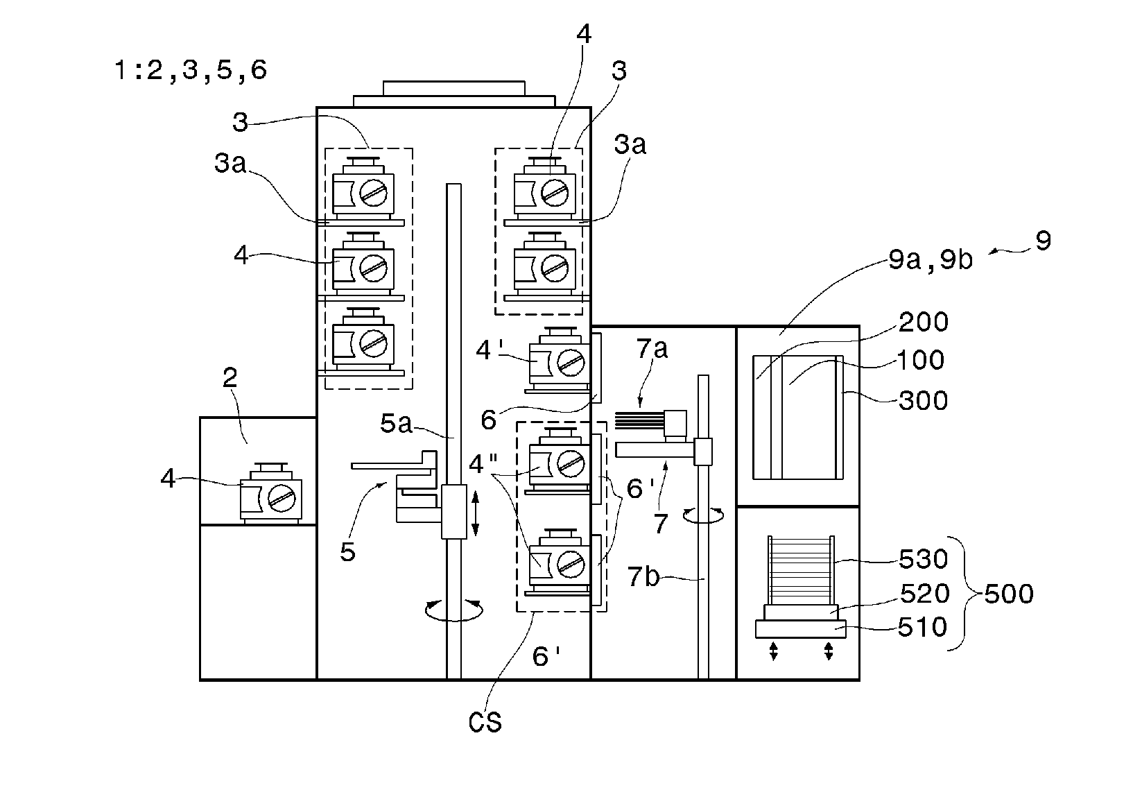
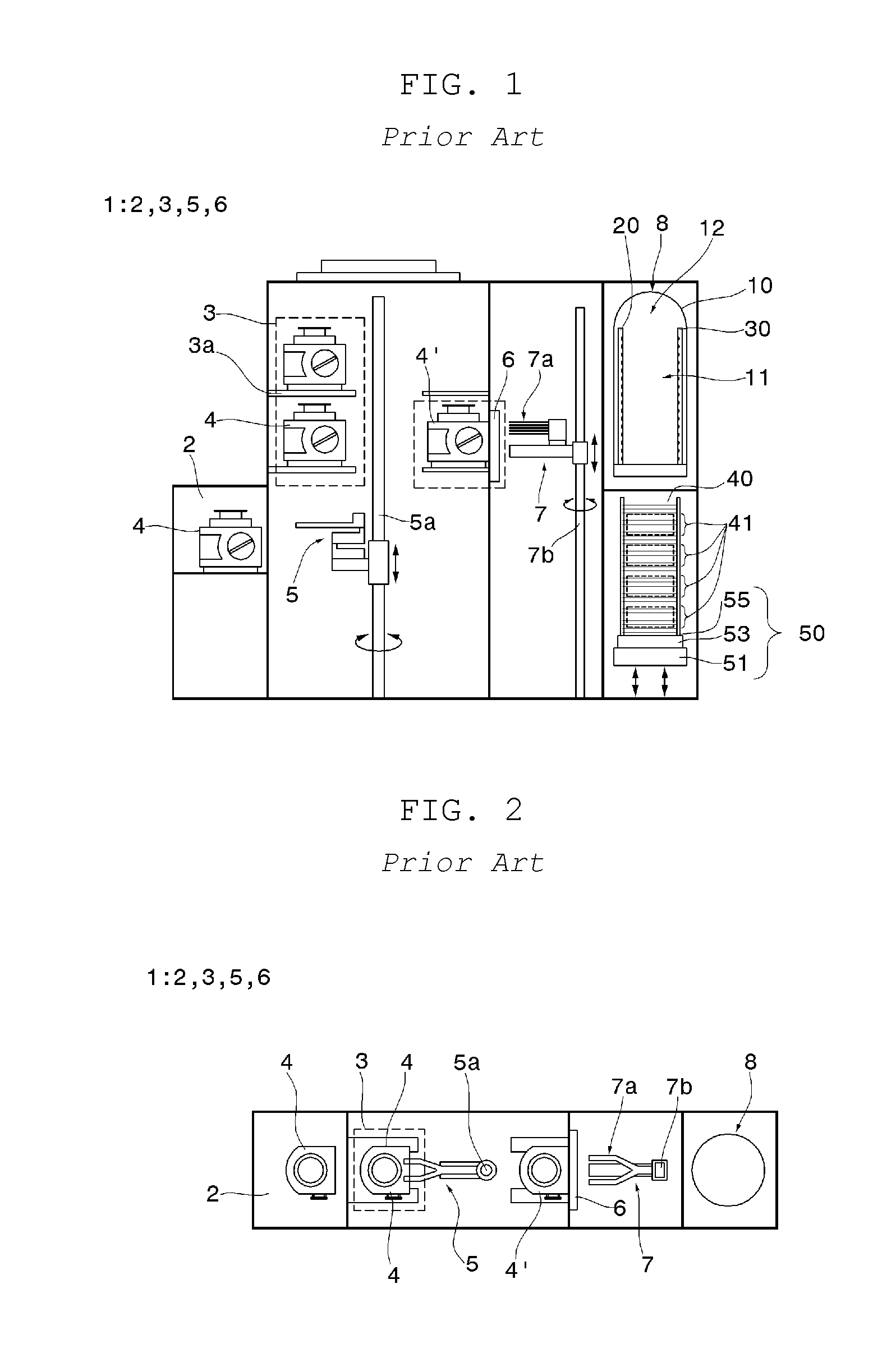
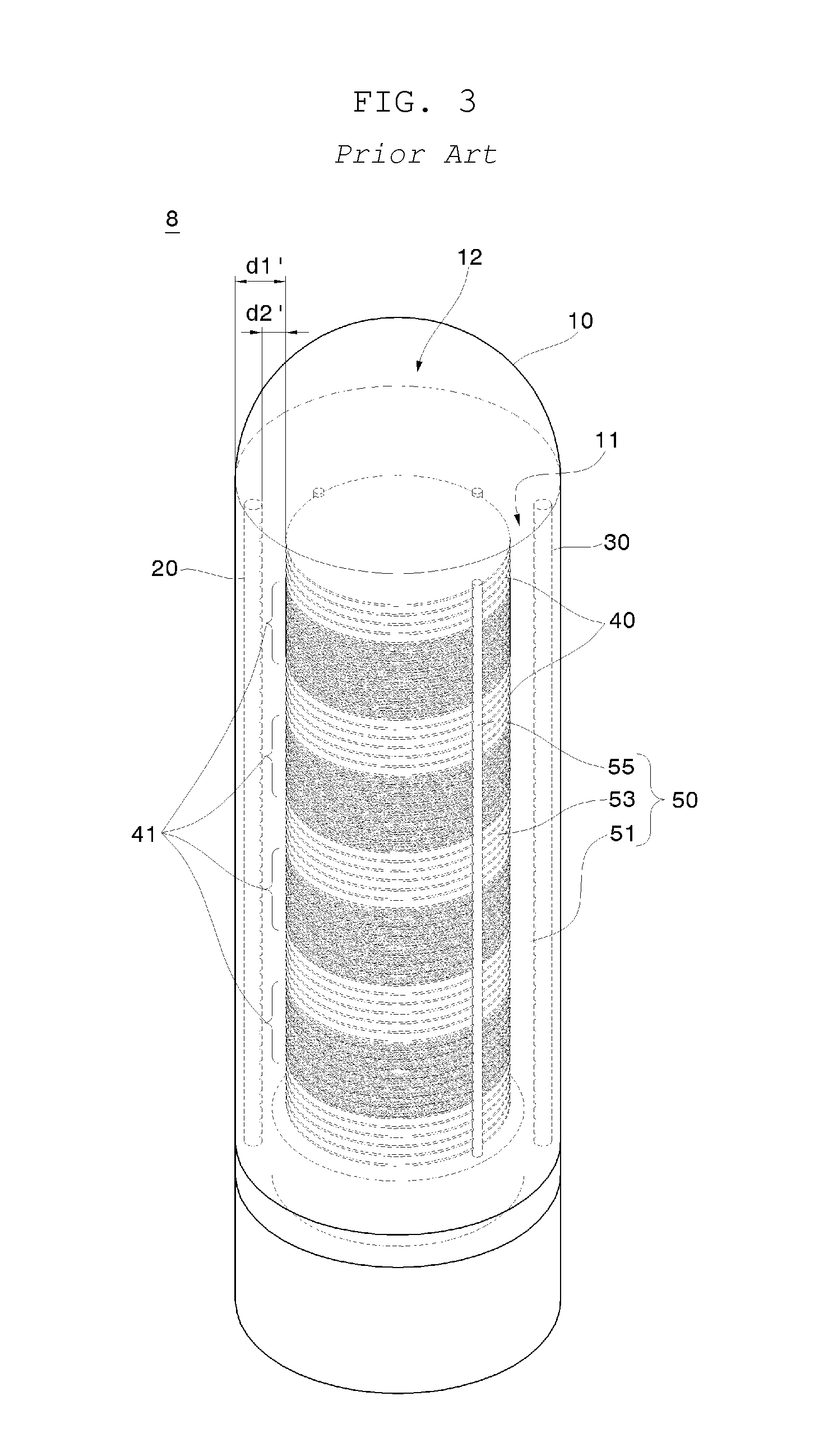
[0036]In the following detailed description of the present invention, references are made to the accompanying drawings that show, by way of illustration, specific embodiments in which the invention may be practiced. These embodiments are described in sufficient detail to enable those skilled in the art to practice the invention. It should be understood that the various embodiments of the invention, although different from each other, are not necessarily mutually exclusive. For example, specific shapes, structures and characteristics described herein may be implemented as modified from one embodiment to another without departing from the spirit and scope of the invention. Moreover, it should be understood that the locations or arrangements of individual elements within each of the disclosed embodiments may be modified without departing from the spirit and scope of the invention. Accordingly, the following detailed description is not to be taken in a limiting sense, and the scope of t...
PUM
| Property | Measurement | Unit |
|---|---|---|
| distance | aaaaa | aaaaa |
| shape | aaaaa | aaaaa |
| adhesiveness | aaaaa | aaaaa |
Abstract
Description
Claims
Application Information