Organic light emitting device

a light-emitting device and organic technology, applied in the direction of solid-state devices, semiconductor devices, thermoelectric devices, etc., can solve the problems of power consumption increase, emission efficiency reduction, brightness and contrast limitations, etc., to enhance illumination, enhance service life, and enhance emission efficiency

Active Publication Date: 2015-05-28
LG DISPLAY CO LTD
View PDF13 Cites 25 Cited by
  • Summary
  • Abstract
  • Description
  • Claims
  • Application Information

AI Technical Summary

Benefits of technology

[0019]An object of the present invention is to provide an organic light emitting device in which emission efficiency is enhanced by using a micro cavity structure.
[0020]Another object of the present invention is to provide an organic light emitting device in which luminance is enhanced by using a micro cavity structure.
[0021]Another object of the present invention is to provide an organic light emitting device in which a service life is enhanced by using a micro cavity structure.

Problems solved by technology

The LCD devices use a backlight as a separate light source, and have technical limitations in brightness and contrast.
However, the method has a problem in which power consumption increases in a case of increasing luminance Also, the method has a problem in which emission efficiency is lowered when a light emitting material is changed for securing a long service life.
However, due to an emission structure of an organic light emitting device, a luminance Cd of a unit area A is limited.
Also, since a current increases for enhancing luminance, a reliability of a device is degraded, and consumption power increases.
Moreover, among pixels of three colors of the organic light emitting device, a blue pixel has a shorter service life than those of a red pixel and a green pixel, and in manufacturing a display panel having the pixels (red, green, and blue pixels) of three colors, a service life of the display panel cannot be ensured.

Method used


Image

  • Organic light emitting device
  • Organic light emitting device
  • Organic light emitting device

Examples


first embodiment

of the Present Invention

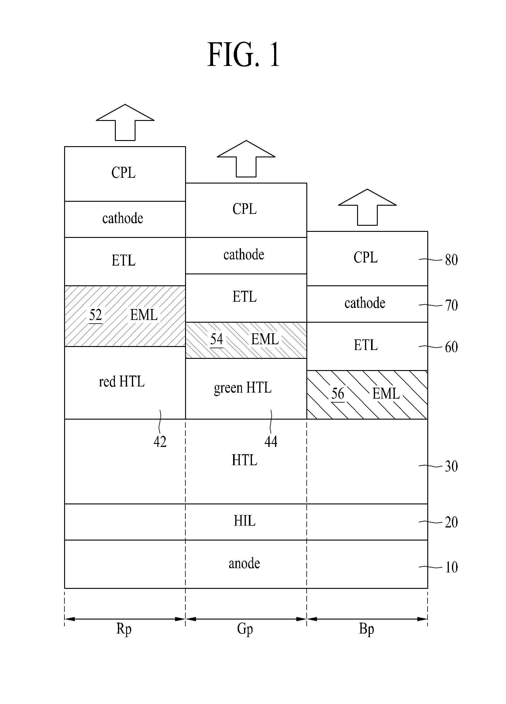
[0067]FIG. 3 is a diagram illustrating red, green, and blue pixel structures of an organic light emitting device 100 according to a first embodiment of the present invention. FIG. 3 illustrates a pixel structure having a top emission type to which a micro cavity structure is applied.

[0068]Referring to FIG. 3, the organic light emitting device 100 according to the first embodiment of the present invention includes a first electrode (an anode electrode) 110, a second electrode (a cathode electrode) 165, and an organic emission layer. The organic light emitting device has a structure in which the organic emission layer is formed between the first electrode (the anode electrode) 110 injecting a positive hole and the second electrode (the cathode electrode) 165 injecting an electron. A capping layer (CPL) 170 is formed on the second electrode (the cathode electrode) 165.

[0069]The organic light emitting device 100 according to the first embodiment of the present in...

second embodiment

of the Present Invention

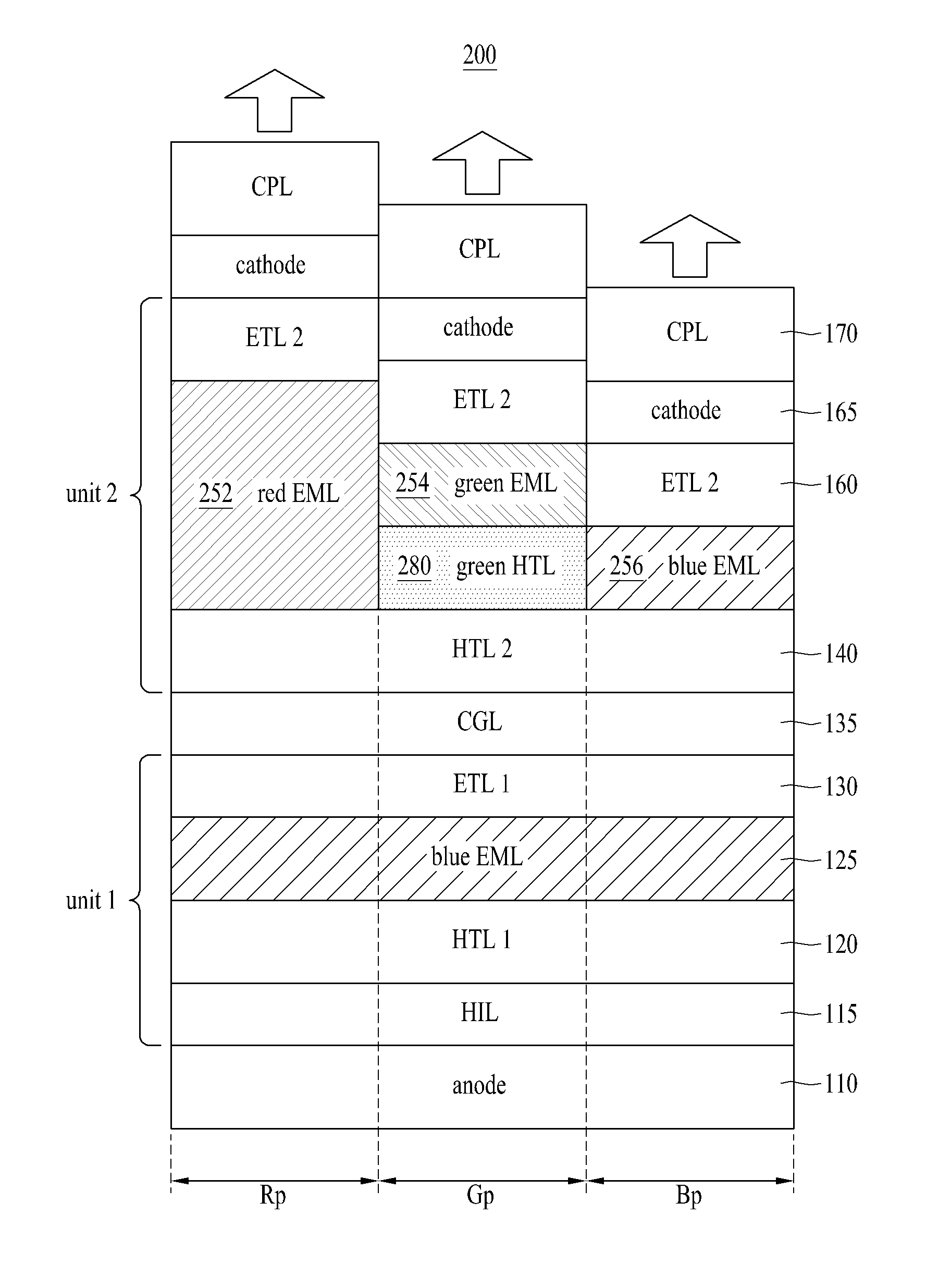
[0131]FIG. 7 is a diagram illustrating red, green, and blue pixel structures of an organic light emitting device 200 according to a second embodiment of the present invention. FIG. 7 illustrates a pixel structure having a top emission type to which a micro cavity structure is applied.

[0132]In describing a pixel structure of the organic light emitting device according to the second embodiment of the present invention, detailed descriptions on the same elements as those of the first embodiment of the present invention described above with reference to FIGS. 3 and 4 may not be provided.

[0133]Referring to FIG. 7, the organic light emitting device 200 according to the second embodiment of the present invention includes a first electrode (an anode electrode) 110, a second electrode (a cathode electrode) 165, and an organic emission layer. The organic light emitting device has a structure in which the organic emission layer is formed between the first electrode (the...

third embodiment

of the Present Invention

[0179]FIG. 9 is a diagram illustrating red, green, and blue pixel structures of an organic light emitting device 300 according to a third embodiment of the present invention. FIG. 9 illustrates a pixel structure having a top emission type to which a micro cavity structure is applied.

[0180]In describing a pixel structure of the organic light emitting device according to the third embodiment of the present invention, detailed descriptions on the same elements as those of the first and second embodiments of the present invention may not be provided.

[0181]Referring to FIG. 9, the organic light emitting device 300 according to the third embodiment of the present invention includes a first electrode (an anode electrode) 110, a second electrode (a cathode electrode) 165, and an organic emission layer. The organic light emitting device has a structure in which the organic emission layer is formed between the first electrode (the anode electrode) 110 injecting a posit...


PUM


Abstract

Disclosed is an organic light emitting device. The organic light emitting device includes a first emission unit configured to include a common blue emission material layer which is included in common in a plurality of pixels emitting lights having different wavelength ranges, a second emission unit configured to include a red emission material layer, a green emission material layer, and a blue emission material layer which respectively emit lights having different wavelength ranges, a charge generation layer disposed between the first emission unit and the second emission unit, a first electrode formed as a reflective electrode, and configured to supply an electric charge having a first polarity to the first emission unit and the second emission unit, and a second electrode formed as a semi-transmissive electrode, and configured to supply an electric charge having a second polarity to the first emission unit and the second emission unit.

Description

CROSS-REFERENCE TO RELATED APPLICATIONS[0001]This application claims the benefit of Korean Patent Application No. 10-2013-0144759 filed on Nov. 26, 2013, which is hereby incorporated by reference as if fully set forth herein.BACKGROUND OF THE INVENTION[0002]1. Field of the Invention[0003]The present invention relates to an organic light emitting device, and more particularly, to an organic light emitting device having a micro cavity emission structure in which emission efficiency and a service life are enhanced.[0004]2. Discussion of the Related Art[0005]To date, liquid crystal display (LCD) devices are being widely used as flat panel display devices. The LCD devices use a backlight as a separate light source, and have technical limitations in brightness and contrast. On the other hand, since organic light emitting devices self-emit light, the organic light emitting devices do not need a separate light source and have relatively better brightness, contrast, and viewing angle, and th...

Claims


Application Information

Patent Timeline
Patent Type & Authority Applications(United States)
IPC IPC(8): H01L51/52H01L51/50
CPCH01L51/5265H01L51/5271H01L51/5072H01L51/5056H01L51/5044H10K59/35H10K50/131H10K50/15H10K50/16H10K50/852H10K50/19H10K50/11H10K50/805
Inventor LEE, SE HEEHWANG, JOO HWANMOON, SANG KYOUNG
Owner LG DISPLAY CO LTD
Why Eureka
Try Eureka