Image sensing device, image reading device, image forming apparatus and image sensing method
- Summary
- Abstract
- Description
- Claims
- Application Information
AI Technical Summary
Benefits of technology
Problems solved by technology
Method used
Image

Examples
first embodiment
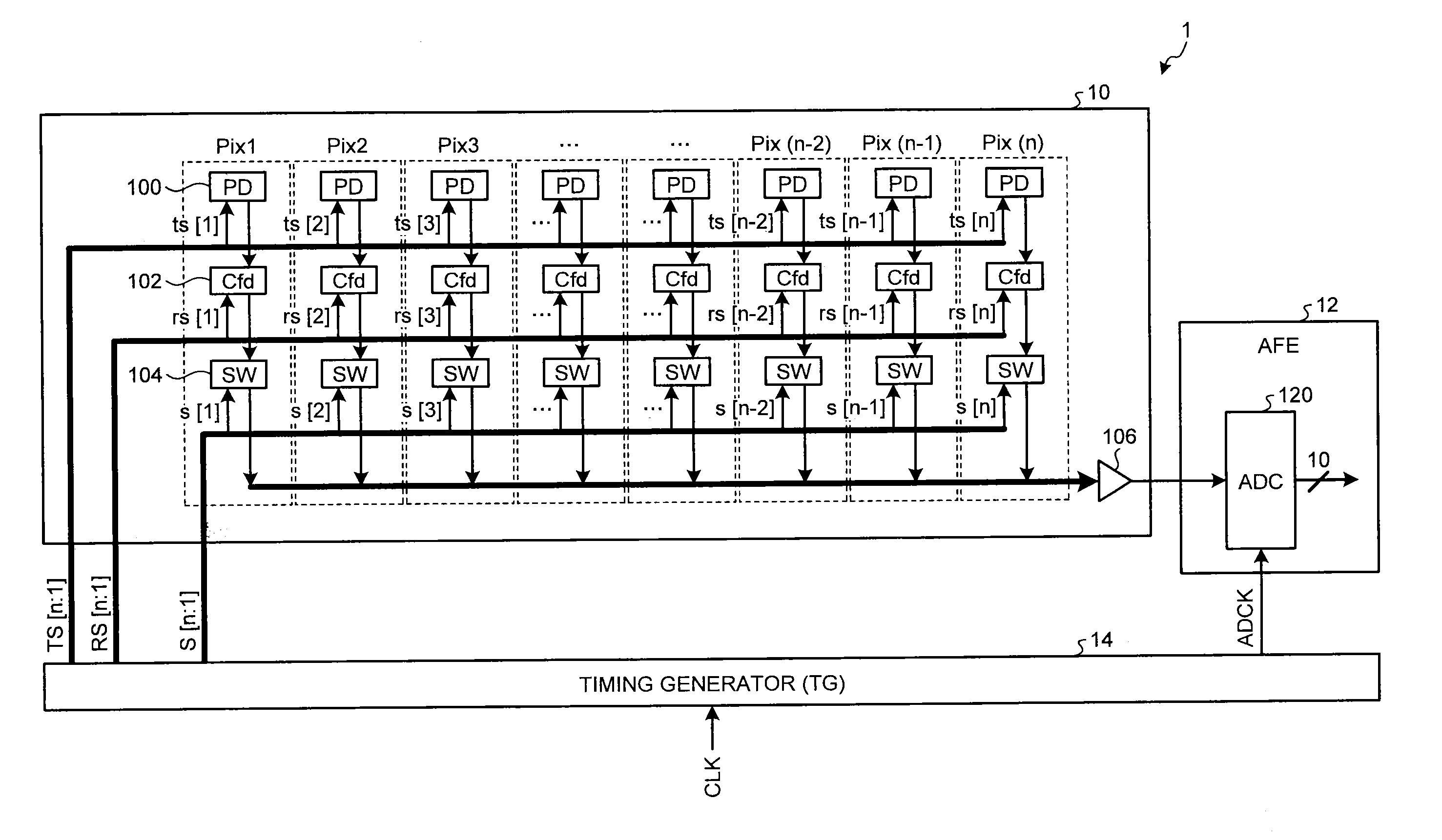
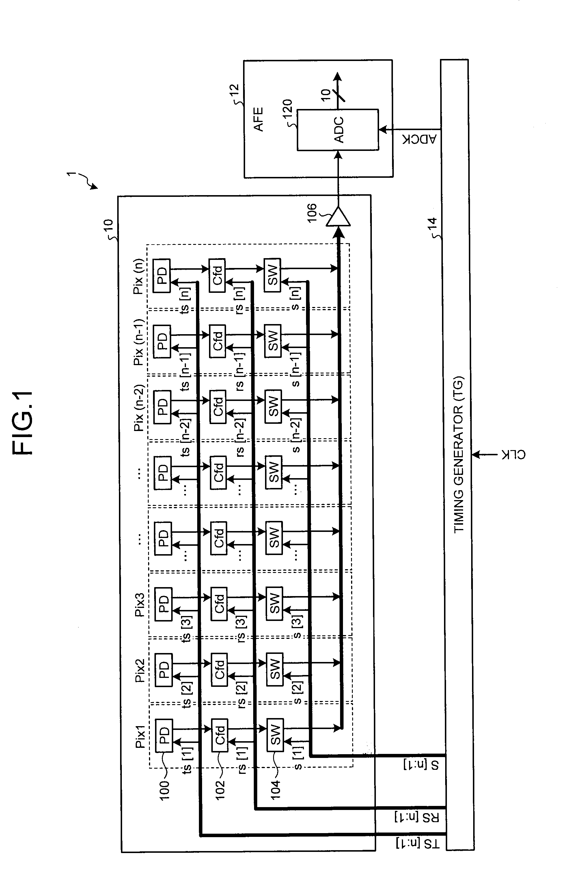
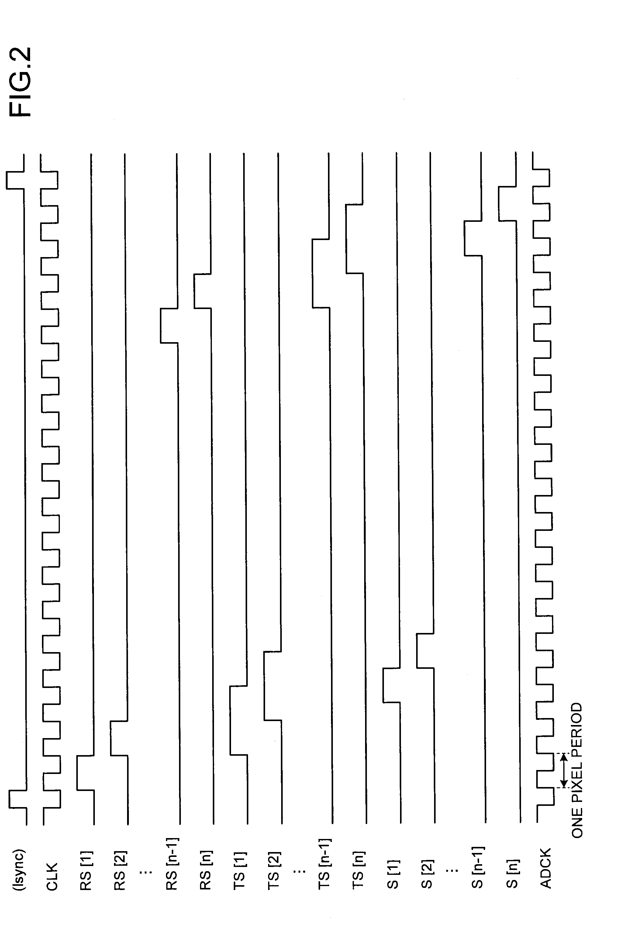
[0050]Described next is an image sensing device according to a first embodiment of the present invention. FIG. 3 is a diagram illustrating an example of a configuration outline of an image sensing device 20 according to the first embodiment. The image sensing device 20 is a CMOS color liner sensor configured to read, for example, Pix1 to Pix(n) that are pixel positions on a subject in the three RGB colors, and includes n pixels (pixel units) in each color arranged in one direction. In the following description, the same reference signs are given to substantially the same constituent elements of each image sensing device.
[0051]A pixel 200 provided with an R filter (not illustrated) includes a photodiode (PD_r) and a pixel block (pixblk_r). A pixel 202 provided with a G filter (not illustrated) includes a photodiode (PD_g) and a pixel block (pixblk_g). A pixel 204 provided with a B filter (not illustrated) includes a photodiode (PD_b) and a pixel block (pixblk_b). Each pixel block inc...
second embodiment
[0074]Described next is an image sensing device according to a second embodiment of the present invention. FIG. 8 is a diagram illustrating an example of a configuration outline of an image sensing device 30 according to the second embodiment. The image sensing device 30 is a CMOS color linear sensor configured to read, for example, Pix1 to Pix(n) that are pixel positions on a subject in the three RGB colors, and includes n pixels (pixel units) in each color arranged in one direction.
[0075]Each pixel group of the image sensing device 20 illustrated in FIG. 3 is composed of three pixels in the same color adjacent to each other arranged in a direction in which pixels in each color are arranged. The pixel groups of the image sensing device 30 are configured differently from those of the image sensing device 20. Each pixel group of the image sensing device 30 is composed of pixels in all colors (pixels surrounded by the black bold line in FIG. 8) configured to read a subject at the same...
third embodiment
[0084]Described next is an image sensing device according to a third embodiment in the present invention. FIG. 12 is a diagram illustrating an example of a configuration outline of an image sensing device 40 according to the third embodiment. FIG. 13 is a diagram illustrating the periphery of an AD converter (ADC) that converts analog signals output from the pixels illustrated in FIG. 12 into digital signals. The image sensing device 40 is configured such that programmable gain amplifiers (PGA) are provided at the preceding stages of the respective ADCs for the pixel groups of the image sensing device 30 illustrated in FIG. 8. Each PGA is configured to change the amplification factor for the PD_*s that constitute a pixel group. The PGAs amplify analog signals output from the pixels 200, the pixels 202, and the pixels 204, whereby the image sensing device 40 can use the dynamic range of the ADCs efficiently.
[0085]The PGAs may amplify the analog signals output from the pixels 200, the...
PUM
 Abstract
Description
Claims
Application Information