Method for determining a characteristic of a surface layer of a fuser element

Inactive Publication Date: 2015-06-18
OCE TECH
View PDF5 Cites 8 Cited by
  • Summary
  • Abstract
  • Description
  • Claims
  • Application Information

AI Technical Summary

Benefits of technology

[0006]It is accordingly an object of the present invention to provide a method for determining a characteristic of a surface layer of a fuser element for fusing a marking ma

Problems solved by technology

The surface layer of the fuser element deteriorates in operation of the printing system due to mechanical wear in the fusing pinch.
Moreover the thickness of the surface layer becomes non-uniform in a direction of the fusing element during use of the fuser element, for example in a dir

Method used


Image

  • Method for determining a characteristic of a surface layer of a fuser element
  • Method for determining a characteristic of a surface layer of a fuser element
  • Method for determining a characteristic of a surface layer of a fuser element

Examples


first embodiment

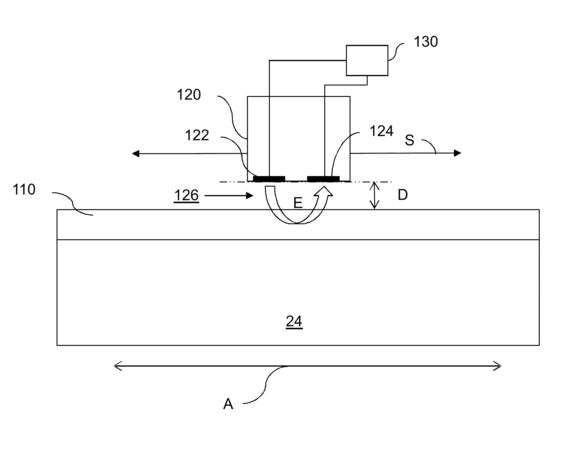
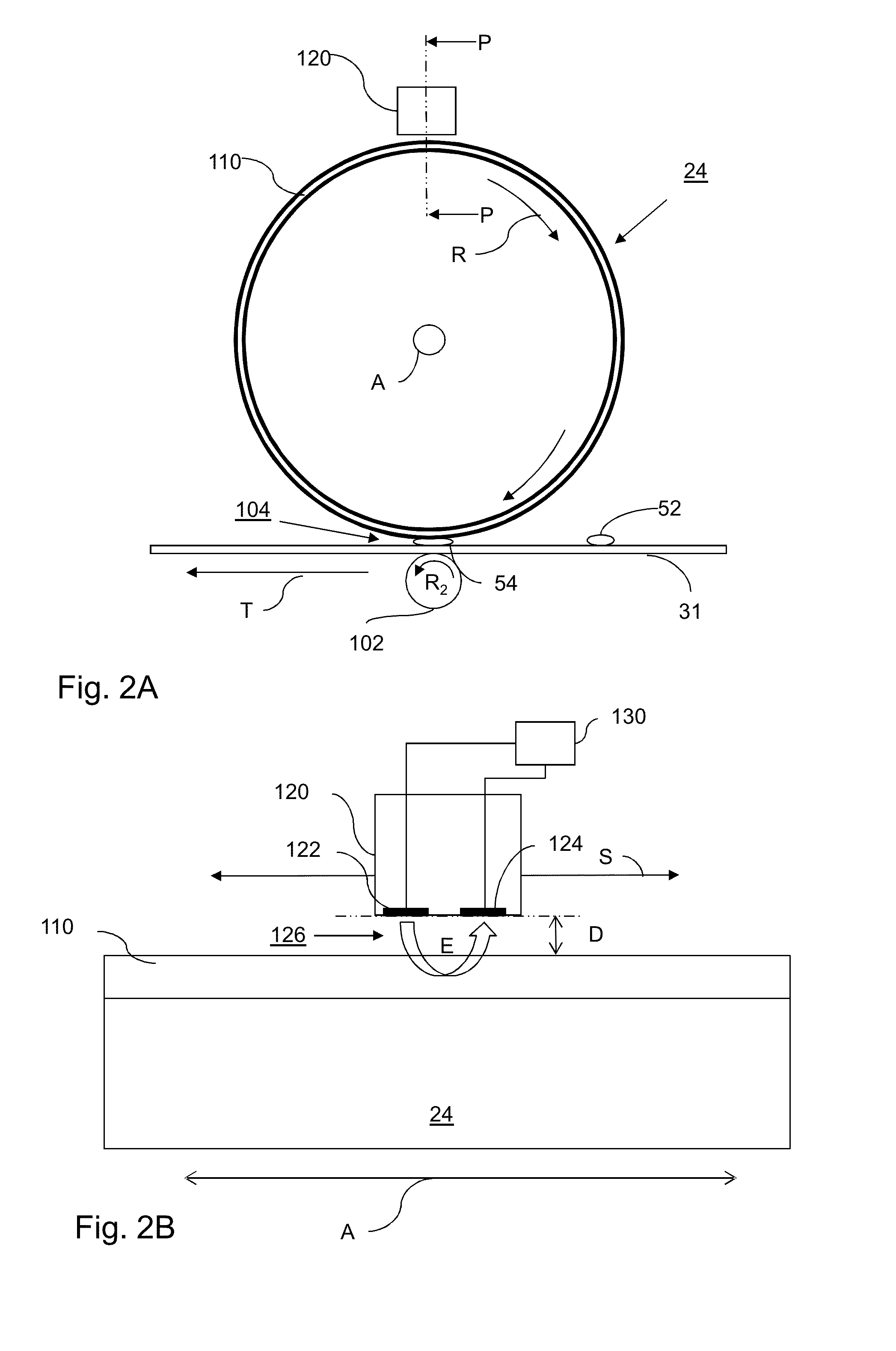
[0070]FIG. 2B shows a cross section view along the line P-P in FIG. 2A of the capacitive probe according to the invention. In FIG. 2B the capacitive probe 120 comprises a first electrode 122 and a second electrode 124. Both first electrode 122 and second electrode 124 are operatively coupled to the capacitive measurement circuit 130. The second electrode 124 is arranged adjacent to the first electrode 122 thereby forming a capacitor. Both the first electrode 122 and the second electrode 124 are plate electrodes, and both electrodes 122, 124 are arranged adjacent to and opposing the surface layer 110 of the fuser roller 24. Both first electrode 122 and second electrode 124 are arranged at a distance D from the surface layer 110 of the fuser roller 24, thereby forming a gap 126, which comprises air, between both first electrode 122 and second electrode 124 and the surface layer 110.

[0071]During a capacitive measurement cycle the potential of the first electrode 122 is changed by a pre...

second embodiment

[0074]FIG. 2C shows a cross section view along the line P-P in FIG. 2A of the capacitive probe according to the invention. The capacitive probe 220 comprises a first electrode 222 and a second electrode 224. The second electrode 224 surrounds the first electrode 222. The first electrode 222 comprises an electric insulating coating 225 in order to electrically decouple the first electrode 222 from the second electrode 224. The first electrode 222 further comprises an uncovered end 223. Both electrodes 222, 224 are operatively coupled to the capacitive measurement circuit 230. The second electrode 224 is arranged adjacent to the end 223 of the first electrode thereby forming a capacitor. Both the end 223 of the first electrode and the second electrode 224 are arranged adjacent to and opposing the surface layer 110 of the fuser roller 24 at a distance D from the surface layer 110 of the fuser roller 24, thereby forming a gap 226, which contains air, between both first electrode 222 and...

third embodiment

[0078]FIG. 2D shows a cross section view along the line P-P in FIG. 2A of the capacitive probe according to the invention. The capacitive probe 240 comprises a first electrode 242 and a second electrode 244. Both first electrode 242 and second electrode 244 are operatively coupled to the capacitive measurement circuit 260. The second electrode 244 is arranged adjacent to the first electrode 242 thereby forming a capacitor. Both the first electrode 242 and the second electrode 244 are plate electrodes, which are both arranged adjacent to and opposing the surface layer 110 of the fuser roller 24. The capacitive probe further comprises a dielectric surface layer 246, which is arranged in between the first and second electrode 242, 244 and the surface layer 110 of the fuser roller 24. The dielectric surface layer has a thickness T. The dielectric surface layer 246 of the capacitive probe is arranged in contact with the surface layer 110.

[0079]The capacitive probe 240 is movably arranged...


PUM


Abstract

The present invention relates to a method for determining a characteristic of a surface layer of a fuser element for fusing a marking material on a recording medium in a printing system. The printing system comprises a capacitive probe, which comprises a first electrode and a second electrode. The second electrode is arranged adjacent to the first electrode in order to form a capacitor. The first electrode and the second electrode are in operation both arranged adjacent to and opposing the surface layer of the fuser element. The method comprises the steps of performing a capacitive measurement on the surface layer by the first electrode and the second electrode of the capacitive probe and determining a characteristic of the surface layer based on the capacitive measurement.

Description

FIELD OF THE INVENTION[0001]The present invention relates to a method for determining a characteristic of a surface layer of a fuser element for fusing a marking material on a recording medium in a printing system. The present invention further relates to a printing system comprising a fuser element and a capacitive probe for determining a characteristic of a surface layer of the fuser element.BACKGROUND OF THE INVENTION[0002]In a known printing system a fuser element is provided for fusing a marking material on a recording medium. The fuser element has a surface layer, which contains an elastomeric compound, configured for providing a uniform pressure to the marking material in a fusing pinch.[0003]The surface layer of the fuser element deteriorates in operation of the printing system due to mechanical wear in the fusing pinch. As a result in the long term a characteristic of the surface layer will change. In general a thickness of the surface layer slowly decreases. Moreover the t...

Claims


Application Information

Patent Timeline
IPC IPC(8): G03G15/20
CPCG03G15/2039G03G15/2053G03G15/553G01B7/085
Inventor VAN HERPEN, WILHELMUS M.NNAFIE, HASSAN
Owner OCE TECH
Why Eureka
Try Eureka