

Method of manufacturing an intermediate product for an interposer and intermediate product for an interposer
a manufacturing method and technology of an interposer, applied in the direction of paper/cardboard containers, printed element electric connection formation, semiconductor/solid-state device details, etc., can solve the problem of difficult to form such fine wiring structures using conventional techniques, and achieve the effect of reducing the risk of cracks and defects
- Summary
- Abstract
- Description
- Claims
- Application Information
AI Technical Summary
Benefits of technology
Problems solved by technology
Method used
Image

Examples
first embodiment
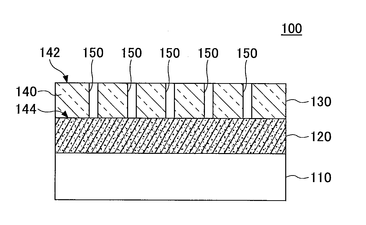
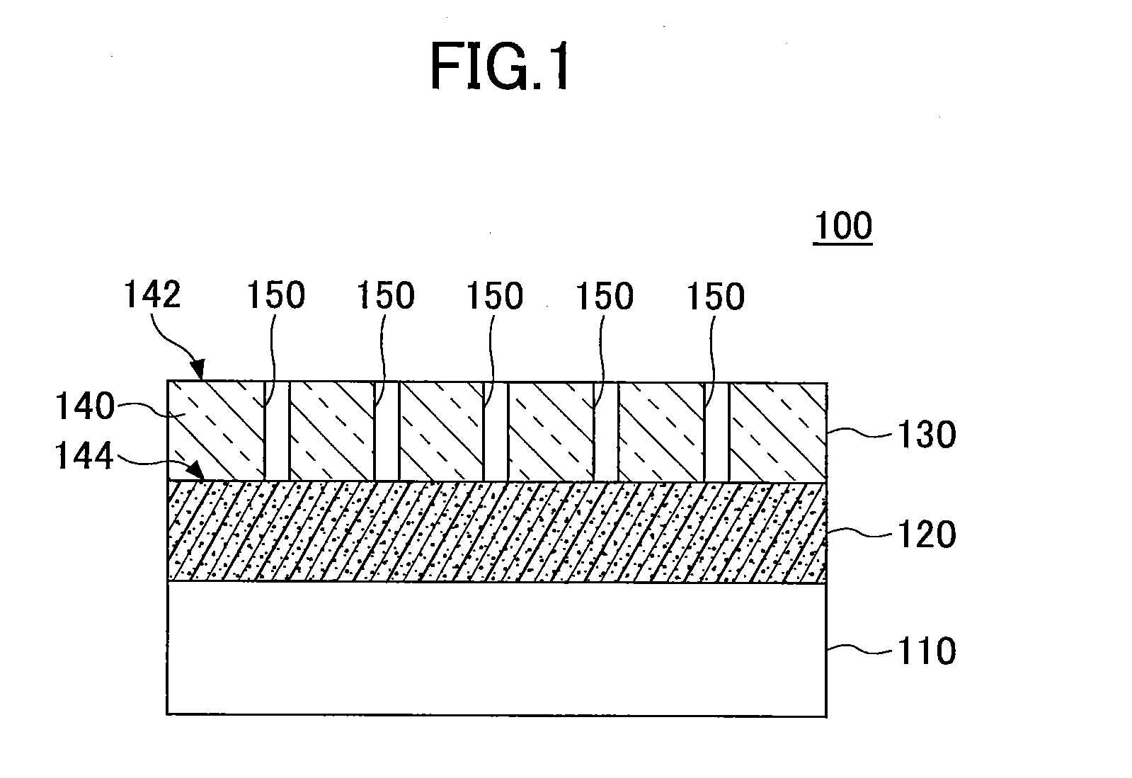
[0055]FIG. 1 is a schematic cross-sectional view of a first laminated body 100 according to the present invention.
[0056]As illustrated in FIG. 1, the first laminated body 100 according to the first embodiment includes a support substrate 110, a resin layer 120, and a glass substrate with through holes 130 stacked in this order.
[0057]The glass substrate with through holes 130 includes a glass substrate 140 with a first surface 142 and a second surface 144 wherein a plurality of through holes 150 penetrating through the first surface 142 and the second surface 144 are formed on the glass substrate 140.
[0058]The glass substrate 140 has a thickness in the range of 0.05 mm to 0.3 mm.
[0059]The support substrate 110 has a greater rigidity than the glass substrate with through holes 130 and is capable of enhancing the strength of the first laminated body 100.
[0060]The resin layer 120 is arranged on the second surface 144 of the glass substrate 140. The resin layer 120 binds the glass substr...
second embodiment
[0085]FIG. 4 is a schematic cross-sectional view of a second laminated body 200 according to the present invention.
[0086]As illustrated in FIG. 4, the second laminated body 200 has a configuration basically similar to that of the laminated body 100 as illustrated in FIG. 1. Thus, in FIG. 4, elements corresponding to those illustrated in FIG. 1 are given reference numerals equal to 100 more than the reference numerals of the corresponding elements in FIG. 1.
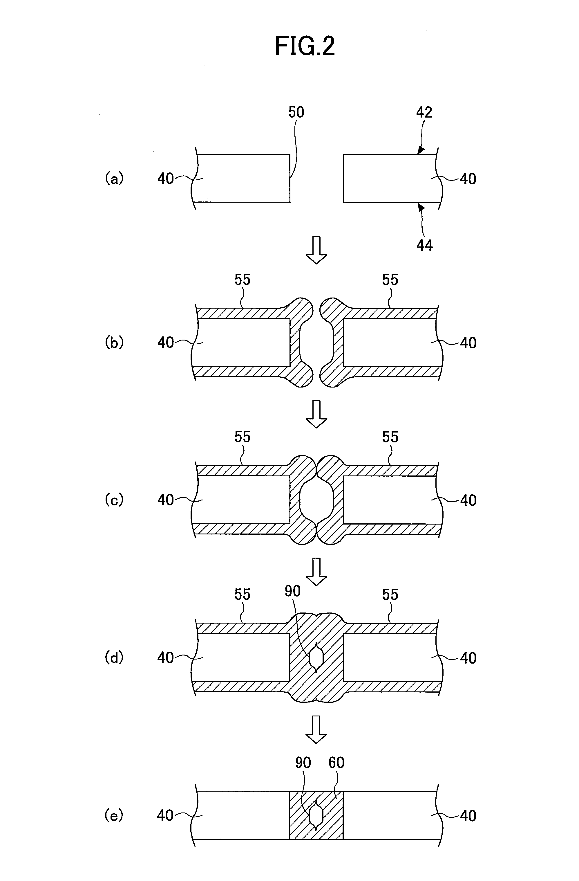
[0087]Note, however, that in contrast to the first laminated body 100, the second laminated body 200 includes via electrodes 260 that are formed by filling a conductive material in through holes 250 of a glass substrate with through-holes 230. Thus, the glass substrate with through-holes 230 of the laminated body 200 also constitutes a glass substrate with via electrodes 230. Note that the type of conductive material filled in the through holes 250 is not particularly limited.
[0088]In the second laminated body 200 having the above...
third embodiment
[0091]FIG. 5 is a schematic cross-sectional view of a third laminated body according to the present invention.
[0092]As illustrated in FIG. 5, the third laminated body 300 has a configuration basically similar to that of the laminated body 200 illustrated in FIG. 4. Thus, in FIG. 5, elements corresponding to those of FIG. 4 are given reference numerals that are equal to 100 more than the reference numerals of the corresponding elements in FIG. 4.
[0093]Note, however, that in contrast to the second laminated body 200, the third laminated body 300 includes a conductive wiring pattern 370 arranged on top of a glass substrate with via electrodes 330.
[0094]The conductive wiring pattern 370 includes an insulating layer 375 and a conductive wiring portion 380 formed inside and on the surface of the insulating layer 375. A part of the conductive wiring portion 380 may be electrically connected to via electrodes 360 of the glass substrate with via electrodes 330.
[0095]In the third laminated bo...
PUM
| Property | Measurement | Unit |
|---|---|---|
| Length | aaaaa | aaaaa |
| Length | aaaaa | aaaaa |
| Thickness | aaaaa | aaaaa |
Abstract
Description
Claims
Application Information