Preventing programming errors from occurring when programming flash memory cells

Active Publication Date: 2015-06-25
SEAGATE TECH LLC
View PDF7 Cites 6 Cited by
  • Summary
  • Abstract
  • Description
  • Claims
  • Application Information

AI Technical Summary

Benefits of technology

[0014]Embodiments of the invention relate to a data storage system, a flash memory IC for use in the data storage system, and methods used therein for preventing programming errors from occurring when programming flash memory. In accordance with an illustrative embodiment, the data storage system comprises a host system and a solid state drive (SSD) that are interfaced with one another. The SSD includes an SSD controller and at least one nonvolatile memory (NVM). The SSD controller includes at least one SSD processor, a tier 1 error-correcting ECC encoder/decoder, and a tier 2 ECC encoder/decoder. The NVM includes at least a first flash memory having a plurality of flash memory cells, reference voltage range determination logic and tier 2 ECC decoding logic. The SSD controller receives write data from the host system to be programmed into flash cells of the NVM. The write data comprises at least a first MSB page of data and at least a first LSB page of data. The tier 1 ECC encoder/decoder performs tier 1 E

Problems solved by technology

Determining or detecting stored data values using controller-provided reference voltages is hampered by undesirable physical non-uniformity across cells of a device that are inevitably introduced by the fabrication process, as such non-uniformity results in the reference voltages of different cells that store the same bit value being significantly different from each other.
The detection is further hampered by target or optimal reference voltages changing over time due to adverse effects of changes in temperature, interference from programming neighboring cells, and numerous erase-program cycles.
The use of error-correcting codes (ECCs) can improve BER to some extent, but the effectiveness of ECCs diminishes as improved fabrication processes result in smaller cell features.
As flash memory technology improves, the sizes of the flash dies scale down, which results in the distance between neighboring flash cells becoming smaller.
Because of the nearness of neighboring flash cells to one another, the

Method used


Image

  • Preventing programming errors from occurring when programming flash memory cells
  • Preventing programming errors from occurring when programming flash memory cells
  • Preventing programming errors from occurring when programming flash memory cells

Examples


Embodiment Construction

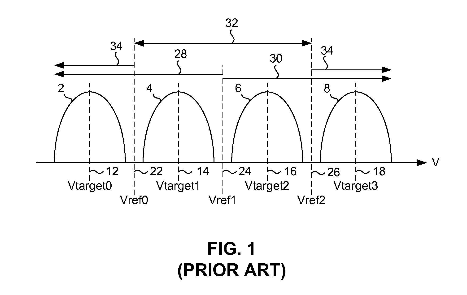
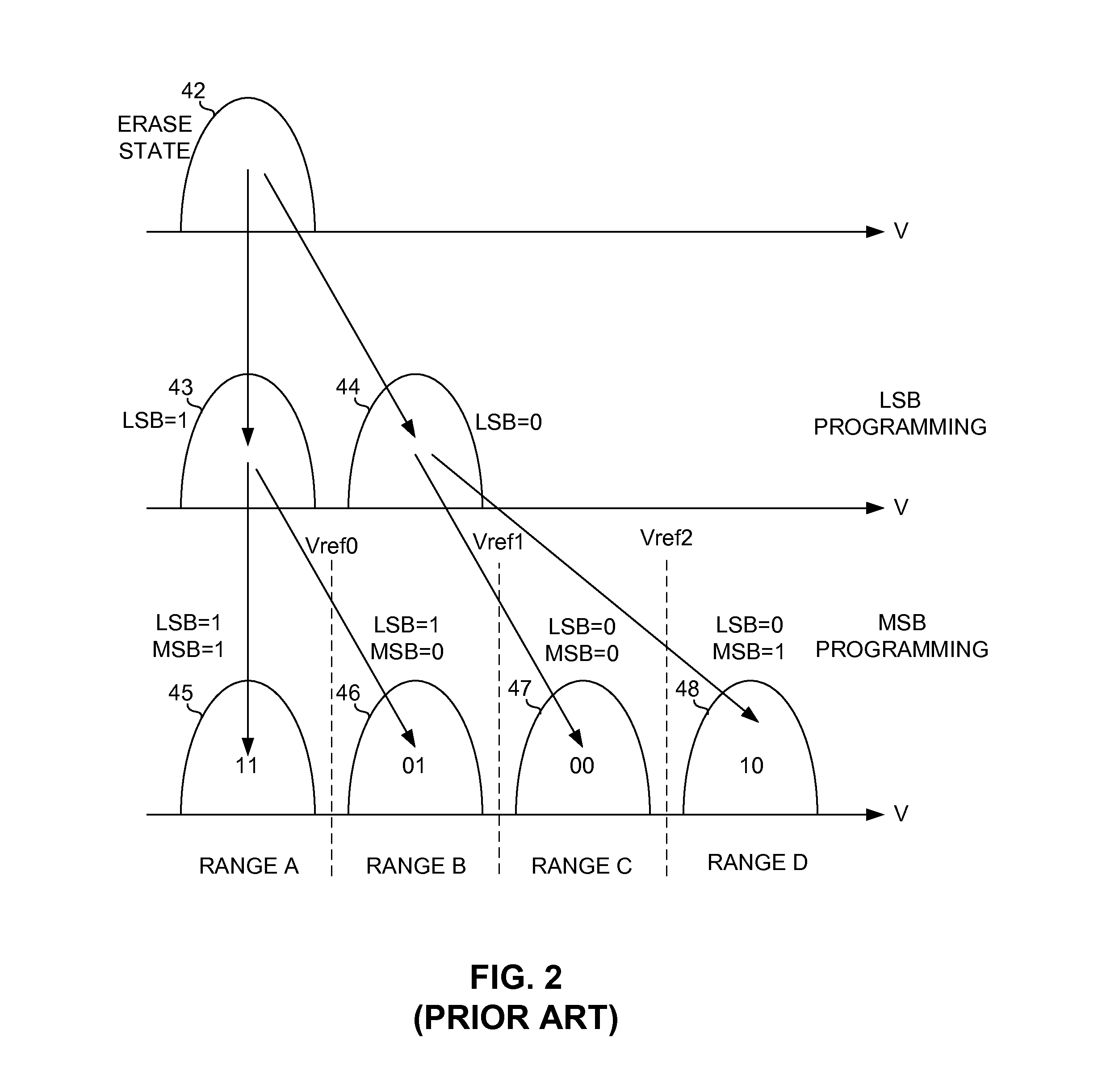
[0026]In accordance with exemplary, or illustrative, embodiments, the LSB values that are used in conjunction with the MSB values to determine the proper reference voltage ranges are error corrected by ECC decoding logic inside of the flash memory before being used in conjunction with the MSB values to determine the proper reference voltage ranges. Error correcting the LSB page data prior to using it in combination with the MSB page data to determine the reference voltage ranges ensures that the reference voltage ranges will be properly determined and programmed into the flash cells.

[0027]Embodiments of the invention can be implemented in a number of ways, and therefore a few illustrative embodiments are described below with reference to FIGS. 3-9, in which like reference numerals in the figures identify like features, components or elements. Before describing specific embodiments for ensuring that programming errors do not occur when programming the reference voltage ranges of the ...


PUM


Abstract

Mis-programming of MSB data in flash memory is prevented by using ECC decoding logic on the flash die that error corrects the LSB values prior to the LSB values being used in conjunction with the MSB values to determine the proper reference voltage ranges. Error correcting the LSB page data prior to using it in combination with the MSB page data to determine the reference voltage ranges ensures that the reference voltage ranges will be properly determined and programmed into the flash cells.

Description

CROSS-REFERENCE TO RELATED APPLICATIONS[0001]This nonprovisional application claims priority to provisional application Ser. No. 61 / 918,778, filed on Dec. 20, 2013, and entitled “PREVENTING PROGRAMMING ERRORS FROM OCCURRING WHEN PROGRAMMING FLASH MEMORY CELLS,” which is incorporated by reference herein in its entirety.TECHNICAL FIELD OF INVENTION[0002]The invention relates generally to flash memory and, more specifically, to preventing programming errors from occurring when programming flash memory cells.BACKGROUND OF THE INVENTION[0003]A flash memory is a non-volatile electrically erasable data storage device that evolved from electrically erasable programmable read-only memory (EEPROM). The two main types of flash memory are named after the logic gates that their storage cells resemble: NAND and NOR. NAND flash memory is commonly used in solid-state drives, which are supplanting magnetic disk drives in many applications. A NAND flash memory is commonly organized as multiple blocks...

Claims


Application Information

Patent Timeline
IPC IPC(8): G06F11/10G11C29/52H03M13/29
CPCG06F11/1068G11C29/52H03M13/29G06F11/1072G11C5/147G11C16/30G11C2029/0411H03M13/1102H03M13/152H03M13/2906H03M13/356
Inventor CAI, YUWU, YUNXIANGCHEN, ZHENGANGHARATSCH, ERICH
Owner SEAGATE TECH LLC
Why Eureka
Try Eureka