Organic light emitting display device and method for driving the same

a light-emitting display and organic technology, applied in the direction of static indicating devices, instruments, etc., can solve the problems of thin film transistor reliability degradation and display panel reliability, and achieve the effect of improving picture quality, reliability and lifespan of switching transistors

Active Publication Date: 2015-07-02
LG DISPLAY CO LTD
View PDF8 Cites 91 Cited by
  • Summary
  • Abstract
  • Description
  • Claims
  • Application Information

AI Technical Summary

Benefits of technology

[0016]An advantage of the present invention is to provide an organic light emitting display device and method for driving the same, in which a variation of driving characteristics of driving transistors may be compensated.
[0017]Another advantage of the present invention is to provide an organic light emitting display device and method for driving the same, in which reliability and lifespan of switching transistors may be increased due to compensation of driving transistors including compensating threshold voltages of driving transistors.
[0018]Other advantage of the present invention is to provide an organic light emitting display device and method for driving the same, in which threshold voltages and / or mobility deviation of driving transistors among pixels may be compensated to improve picture quality.
[0019]Additional features and advantages of the invention will be set forth in the description which follows, and in part will be apparent from the description, or may be learned by practice of the invention. These and other advantages of the invention will be realized and attained by the structure particularly pointed out in the written description and claims hereof as well as the appended drawings.
[0020]To achieve these objects and other advantages and in accordance with the purpose of the invention, as embodied and broadly described herein, an organic light emitting display device may include a display panel having a plurality of pixels, each pixel connected to a data line, a gate line group and a reference line, each pixel further including: an organic light emitting device; a driving transistor controlling a current flowing in the organic light emitting device and including first and second gate electrodes overlapped with each other, with a semiconductor layer provided therebetween; a first switching transistor selectively supplying a data voltage supplied to the data line to a first node connected to the first gate electrode; a second switching transistor selectively supplying a sensing voltage to the second gate electrode; a third switching transistor selectively connecting a second node connected to a source electrode of the driving transistor to the first node; a fourth switching transistor selectively connecting the reference line to the second node; a first capacitor connected between the second gate electrode and the second node, the first capacitor storing a threshold voltage of the driving transistor; and a second capacitor connected between the first and second nodes, the second capacitor storing a difference voltage of the first and second nodes.
[0021]In another aspect of the present invention, an organic light emitting display device may include a pixel connected to a data line, a gate line group and a reference line, the pixel comprising an organic light emitting device; a driving transistor controlling a current flowing in the organic light emitting device and including first and second gate electrodes overlapped with each other by interposing a semiconductor layer therebetween; a first capacitor connected between the second gate electrode and a source electrode of the driving transistor; a second capacitor connected between the first gate electrode and the source electrode; and a switching unit switched in accordance with a control signal supplied to the gate line group, storing a threshold voltage of the driving transistor in the first capacitor, storing a difference voltage of a data voltage supplied to the data line and a reference voltage supplied to the reference line in the second capacitor, and allowing the light emitting device to emit light by driving the driving transistor through voltages of the first and second capacitors.

Problems solved by technology

However, in the general organic light emitting display device, threshold voltages Vth of the transistors Tdr and Tsw, especially the driving transistor Tdr, are different for each pixel due to non-uniformity caused by the manufacturing processes of the thin film transistors.
Accordingly, in the general organic light emitting display device, reliability of the thin film transistors and the display panel deteriorates due to such an initial non-uniformity of the threshold voltages of the thin film transistors included in each pixel or a shift of the threshold voltages according to lapse of time.

Method used


Image

  • Organic light emitting display device and method for driving the same
  • Organic light emitting display device and method for driving the same
  • Organic light emitting display device and method for driving the same

Examples


first embodiment

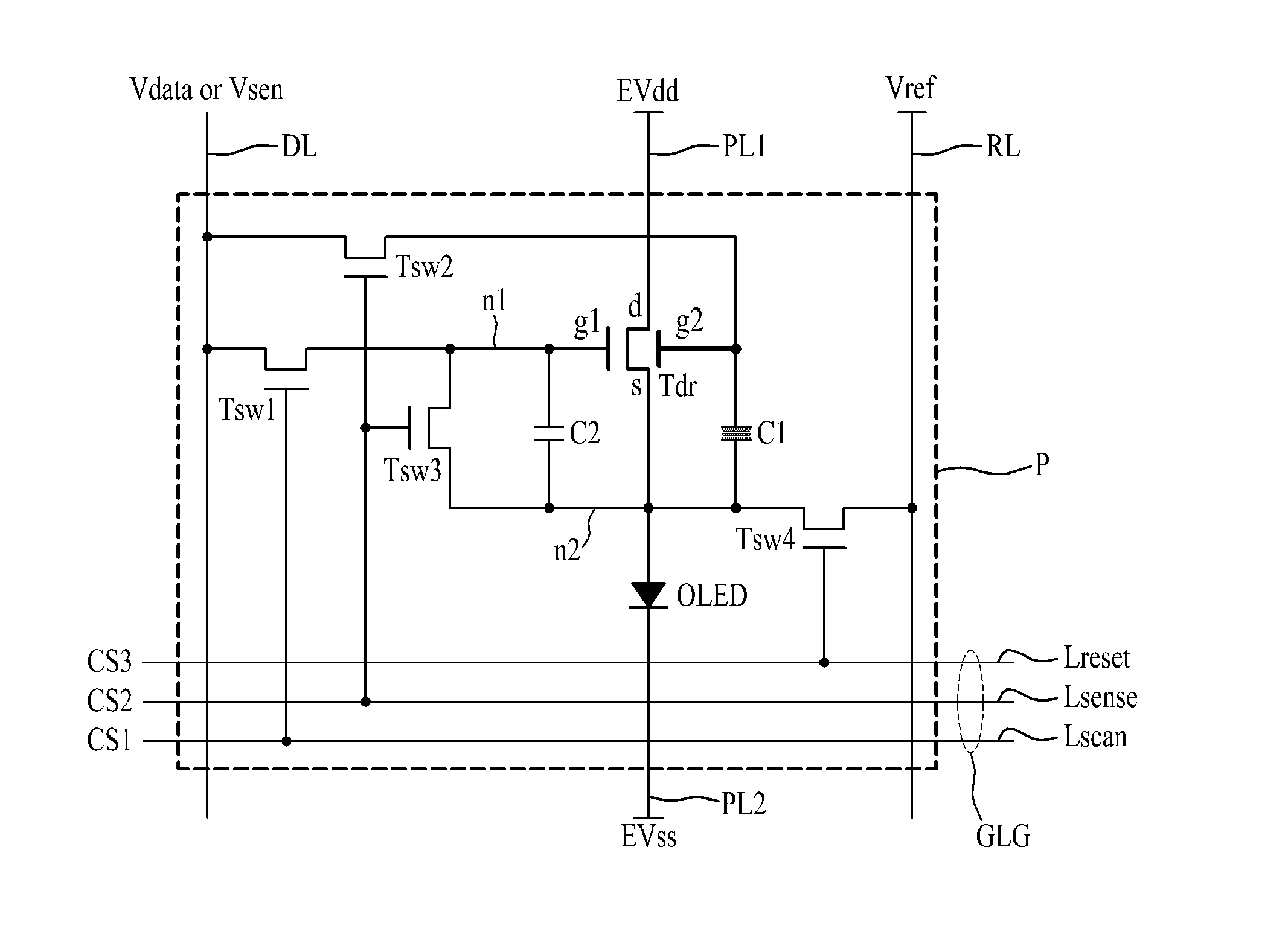
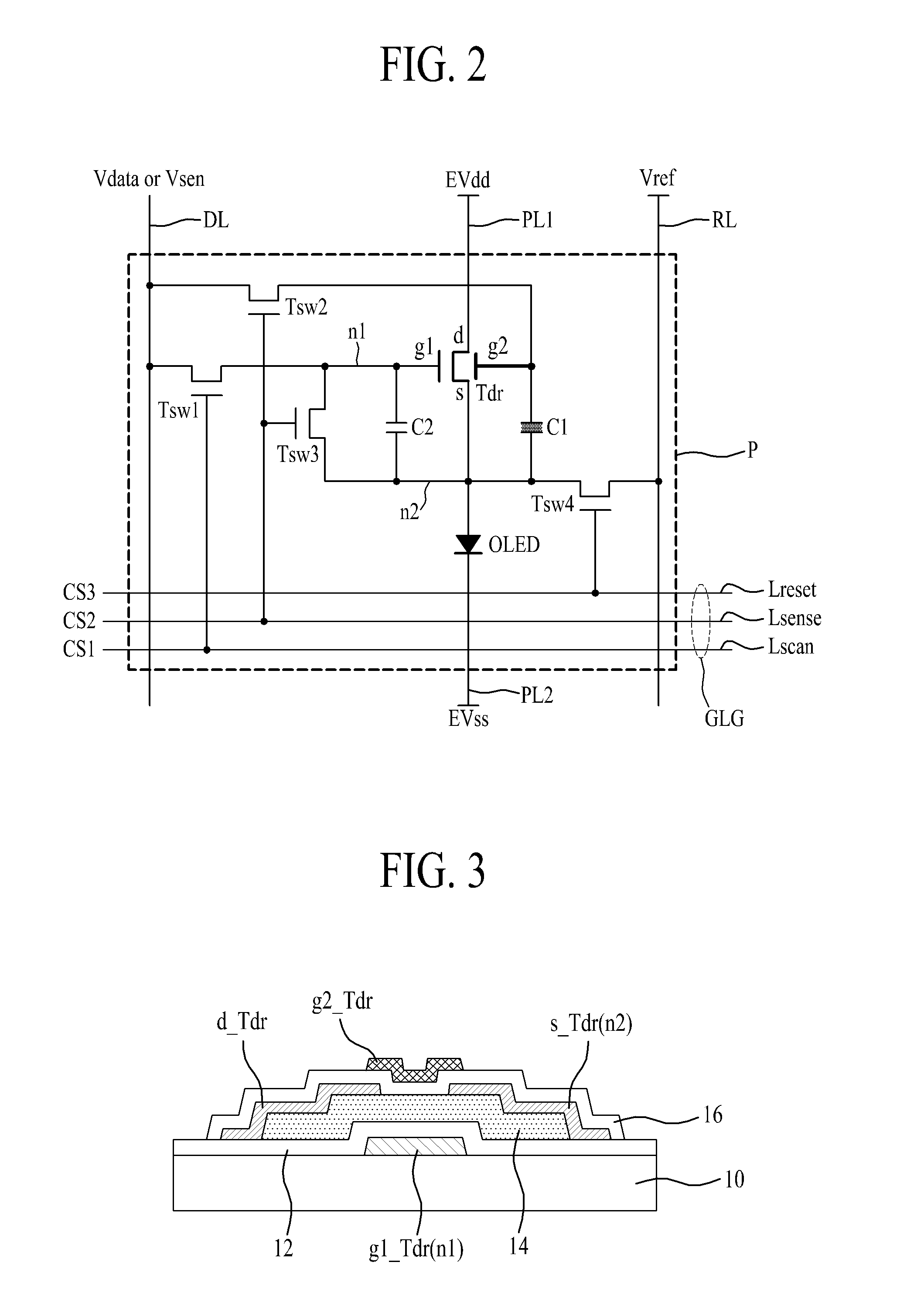
[0048]FIG. 2 is a circuit diagram illustrating a pixel structure of an organic light emitting display device according to the present invention. FIG. 3 is a cross-sectional view illustrating a structure of a driving transistor shown in FIG. 2

[0049]Referring to FIGS. 2 and 3, a pixel P is connected to a data line DL, a gate line group GLG, a reference line RL, a first driving power line PL1, and a second driving power line PL2.

[0050]The data line DL is formed along a first direction of a display panel (not shown), for example, a vertical direction. A data voltage Vdata from a data driver (not shown) is supplied to the data line DL.

[0051]The gate line group GLG is formed along a second direction of the display panel, for example, a horizontal direction to cross the data line DL. The gate line group GLG includes a scan control line Lscan, a sensing control line Lsense, and a reset control line Lreset.

[0052]The reference line RL is formed to be parallel with the data line DL. The refere...

second embodiment

[0101]The pixel P according to external compensation driving of the second embodiment may include the reset period t1 shown in FIG. 4A, the data addressing period AP shown in FIG. 5A or FIG. 5C, and the light emitting period EP shown in FIG. 5B.

[0102]During the data addressing period AP of the external compensation driving according to the first and second embodiments, the data voltage converted from the corrected data corrected based on the sensing data Sdata, that is, the data voltage that includes a compensation voltage for compensating the threshold voltage of the driving transistor Tdr is supplied to the corresponding data line.

[0103]FIG. 7 is a diagram illustrating a structure of a pixel according to the second embodiment of the present invention, wherein a sensing voltage line for supplying a sensing voltage is additionally provided in a second switching transistor.

[0104]As described above, in the pixel P according to the first embodiment of the present invention, the first e...

third embodiment

[0107]FIG. 8 is a diagram illustrating a structure of a pixel according to the present invention, wherein a connection structure of first and second gate electrodes of the driving transistor Tdr is changed. Hereinafter, only different elements will be described.

[0108]As described above, in the pixel P according to the first embodiment of the present invention, the first gate electrode g1 of the driving transistor Tdr is connected to the first and third switching transistors Tsw1 and Tsw3 and the second capacitor C2 through the first node n1, and the second gate electrode g2 of the driving transistor Tdr is connected to the second switching transistor Tsw2 and the first capacitor C1.

[0109]On the other hand, as illustrated in FIG. 8, in the structure of the pixel P according to the third embodiment of the present invention, positions of the first and second gate electrodes g1 and g2 of the driving transistor Tdr are exchanged. In other words, the first gate electrode g1 of the driving...


PUM


Abstract

An organic light emitting display device includes a display panel having a plurality of pixels, each pixel connected to a data line, a gate line group and a reference line, each pixel further including: an organic light emitting device; a driving transistor controlling a current flowing in the organic light emitting device and including first and second gate electrodes overlapped with each other, with a semiconductor layer provided therebetween; a first switching transistor selectively supplying a data voltage supplied to the data line to a first node connected to the first gate electrode; a second switching transistor selectively supplying a sensing voltage to the second gate electrode; a third switching transistor selectively connecting a second node connected to a source electrode of the driving transistor to the first node; a fourth switching transistor selectively connecting the reference line to the second node; a first capacitor connected between the second gate electrode and the second node, the first capacitor storing a threshold voltage of the driving transistor; and a second capacitor connected between the first and second nodes, the second capacitor storing a difference voltage of the first and second nodes.

Description

CROSS REFERENCE TO RELATED APPLICATIONS[0001]This application claims the benefit of Korean Patent Application No. 10-2013-0166471, filed on Dec. 30, 2013, which is hereby incorporated by reference for all purposes as if fully set forth herein.BACKGROUND OF THE INVENTION[0002]1. Field of the Invention[0003]The present invention relates to a flat panel display device, and more particularly, to an organic light emitting display device that includes a thin film transistor.[0004]2. Discussion of the Related Art[0005]Recently, with the development of information society, flat panel display devices having characteristics such as slimness, lightweight, and low power consumption have been in demand. Among various types of flat panel display devices, liquid crystal display devices and organic light emitting display devices, each of which includes an array of thin film transistors, have been widely commercialized as display devices for televisions, notebook computers, tablet computers or deskt...

Claims


Application Information

Patent Timeline
Patent Type & Authority Applications(United States)
IPC IPC(8): G09G3/32
CPCG09G3/3291G09G2310/0264G09G2320/0219G09G3/3233G09G2300/0426G09G2300/0814G09G2300/0819G09G2300/0852G09G2310/0251G09G2320/0233G09G3/32
Inventor SHIM, JONG SIKBAE, NA YOUNG
Owner LG DISPLAY CO LTD
Why Eureka
Try Eureka