

Light emitting diode package structure
- Summary
- Abstract
- Description
- Claims
- Application Information
AI Technical Summary
Benefits of technology
Problems solved by technology
Method used
Image

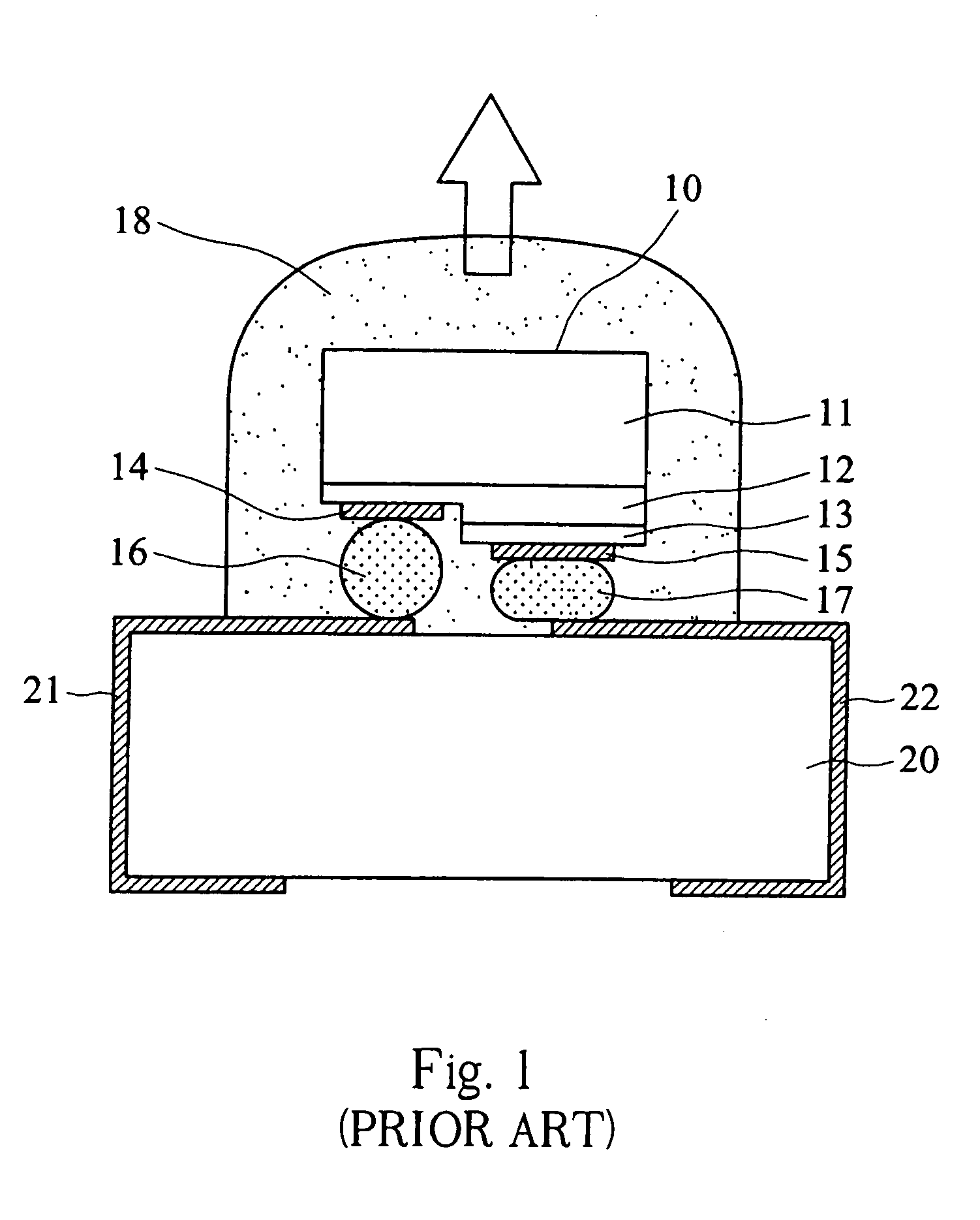
Examples
first embodiment
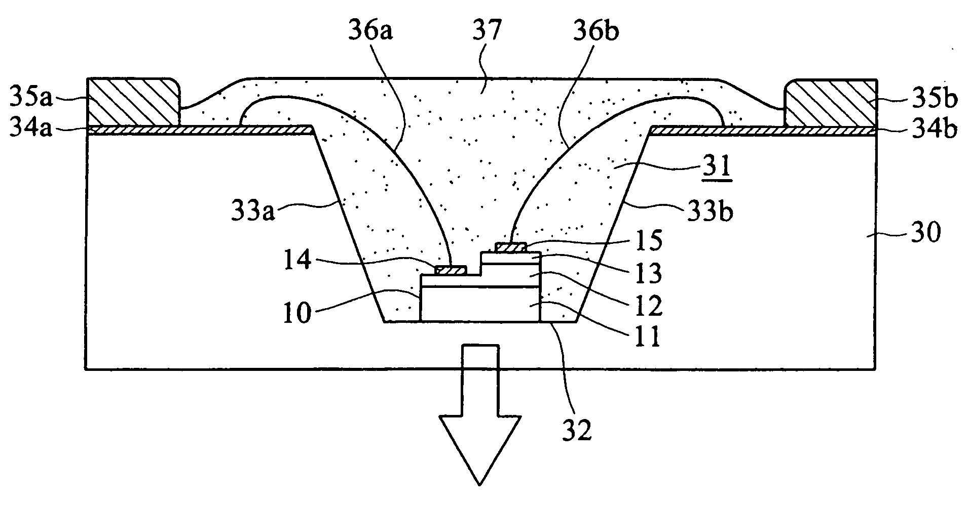
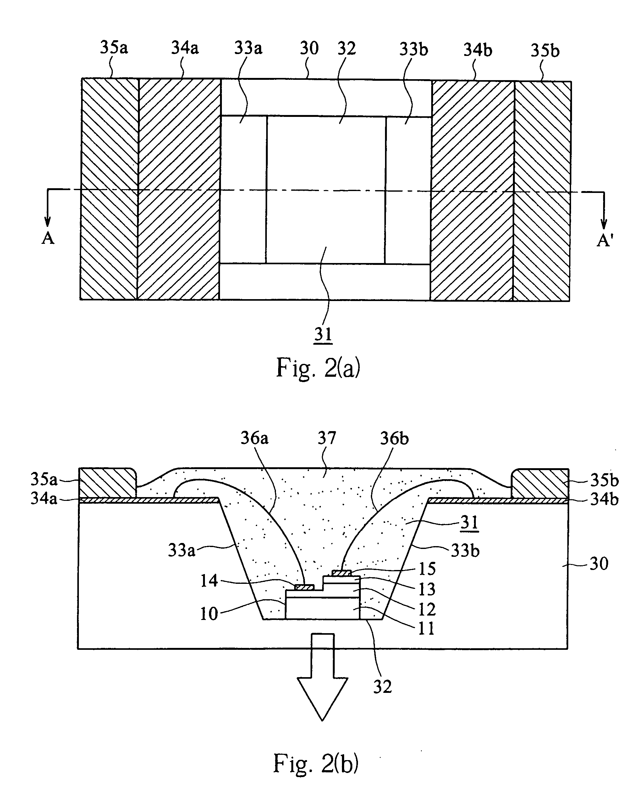
[0027]FIG. 2(a) is a top plan view showing a transparent insulating carrier base 30 according to the present invention while FIG. 2(b) is a cross-sectional view showing a light emitting diode package structure taken along a line A-A′ of FIG. 2(a). Referring to FIG. 2(a), the transparent insulating carrier base 30 is formed with a recess 31 in an approximately central region thereof. The recess 31 has a bottom surface 32 and two sidewall surfaces 33a and 33b. For example, the transparent insulating carrier base 30 is made of glass. Two planar metal layers 34a and 34b, which are separated from each other, are formed in a region other than the recess 31 on the top surface of the transparent insulating carrier base 30. In addition, two metal pads 35a and 35b are formed on the planar metal layers 34a and 34b to locate in peripheral regions of the transparent insulating carrier base 30.
[0028] Referring to FIG. 2(b), the light emitting diode 10 is delivered into the recess 31 such that the...
third embodiment
[0038] When a power supply is applied to the light emitting diode 10 through the protruding metal pads 35a and 35b, the light emitting diode 10 radiates light to external space through the substrate 11 and the transparent resin 53a, as indicated by an arrow of FIG. 4. Since it is not necessary for the light to transmit through the insulating carrier base 50 to external space, the insulating carrier base 50 of the third embodiment is not limited to being made of a transparent material such as glass; it may be made of ceramic, AlN, SiC, plastic, resin, a printed circuit board, or a combination thereof. In addition, the insulating carrier base 50 may be a combination of a plurality of elements, such as a metal core body coated with an insulating material outer film.
[0039]FIG. 5 is a cross-sectional view showing a light emitting diode package structure according to a fourth embodiment of the present invention. Hereinafter only described are differences of the fourth embodiment from the ...
fifth embodiment
[0044] In the fifth embodiment, a lower resin portion 73a and an upper resin portion 73b are used for sealing all of the light emitting diode 10 and the wirings 36a and 36b. The lower resin portion 73a is made of a transparent material and serves as a light-transmitting channel. Preferably, the lower resin portion 73a is made of a material having a refraction index which matches the refraction index of the substrate 11 in such a manner that the total reflection between the substrate 11 and the lower resin portion 73a is reduced. The upper resin portion 73b may be made of a reflective material or a resin doped with a reflective material and serves to reflect the light toward the lower resin portion 73a. In addition, in order to further enhance the lighting efficiency, a reflective layer (not shown) may be coated on the upper resin portion 73b for causing the light generated from the light emitting diode 10 to be reflected toward the lower opening 52a. Moreover, an optical lens 74 may...
PUM
 Abstract
Description
Claims
Application Information