Substrate processing apparatus, method of manufacturing semiconductor device, and non-transitory computer-readable recording medium

Inactive Publication Date: 2015-07-02
KOKUSA ELECTRIC CO LTD
View PDF4 Cites 14 Cited by
  • Summary
  • Abstract
  • Description
  • Claims
  • Application Information

AI Technical Summary

Benefits of technology

[0008]It is an object of the present invention to provide a substrate processing apparatus which prevents operations of a vacuum pump provided in

Problems solved by technology

If the pressure on the downstream side of the vacuum pump rises due to some reasons, a gas flows back to

Method used


Image

  • Substrate processing apparatus, method of manufacturing semiconductor device, and non-transitory computer-readable recording medium
  • Substrate processing apparatus, method of manufacturing semiconductor device, and non-transitory computer-readable recording medium
  • Substrate processing apparatus, method of manufacturing semiconductor device, and non-transitory computer-readable recording medium

Examples


first embodiment

[0021]Hereinafter, the present invention will be described with reference to the accompanying drawings.

[0022][Configuration of Apparatus]

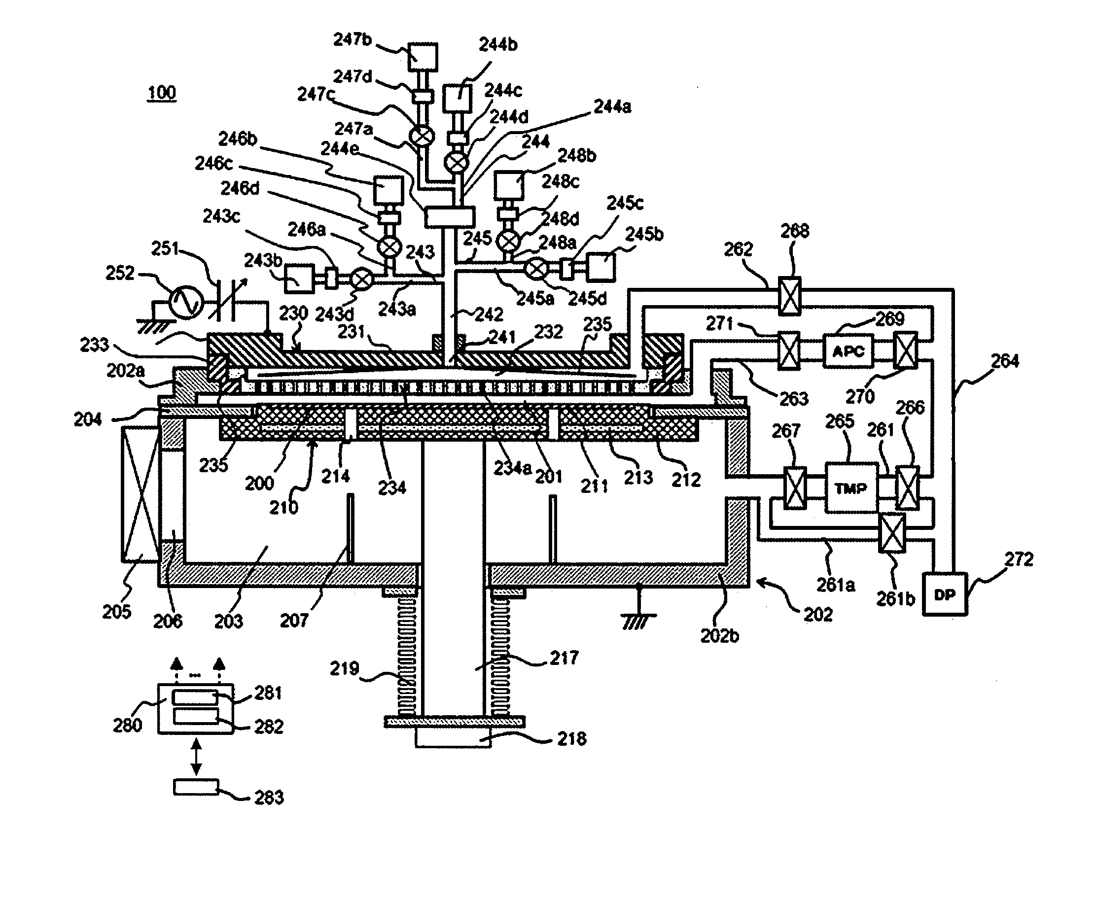
[0023]A configuration of substrate processing apparatus 100 according to an embodiment of the present invention is shown in FIG. 1. The substrate processing apparatus 100 is configured as a batch-type substrate processing apparatus as shown in FIG. 1.

[0024][Processing Container]

[0025]The substrate processing apparatus 100 includes a processing container 202 as shown in FIG. 1. The processing container 202 is configured as a flat sealed container whose cross-sectional surface has, for example, a circular shape. In addition, the processing container 202 is made of a metal material such as aluminum (Al), stainless steel (SUS), or the like. A processing space 201 that processes a wafer 200 such as a silicon wafer or the like as a substrate and a transfer space 203 through which the wafer 200 passes when the wafer 200 is transferred to the processing sp...

second embodiment

[0128]Next, the present invention will be described.

[0129][Apparatus Configuration]

[0130]A substrate processing apparatus 102 according to the second embodiment is shown in FIG. 5. In addition, the same reference numerals are used to designate the same configurations as in the substrate processing apparatus 100 according to the first embodiment, and thus description thereof will be omitted.

[0131]In the substrate processing apparatus 102 according to the second embodiment, an inert gas supply unit that supplies N2 gas between the TMP 265 and the valve 267 upstream from the TMP 265 in the exhaust pipe 261 is provided. The inert gas supply unit includes a supply pipe 290, an inert gas supply source 291 connected to the downstream side of the supply pipe 290, a valve 292 provided upstream from the inert gas supply source 291 in the supply pipe 290, and a mass flow controller (MFC) 293 which is provided between the inert gas supply source 291 and the valve 292 in the supply pipe 290. The...


PUM

PropertyMeasurementUnit
Pressureaaaaaaaaaa
Flow rateaaaaaaaaaa

Abstract

A substrate processing apparatus processes a substrate by supplying a gas into a processing space. The apparatus includes a buffer space wherein the gas is dispersed, the buffer space disposed at an upstream side of the processing space; a transfer space where the substrate passes when transferred to the processing space; a first, a second and a third exhaust pipe connected to the transfer space, the buffer space and the processing space, respectively; a fourth exhaust pipe connected to downstream sides of the first exhaust pipe, the second exhaust pipe and the third exhaust pipe; a first vacuum pump disposed at the first exhaust pipe; a second vacuum pump disposed at the fourth exhaust pipe; a first valve disposed at the first exhaust pipe at a downstream side of the first vacuum pump; and a second and a third valve disposed at the second and the third exhaust pipe, respectively.

Description

CROSS-REFERENCE TO RELATED PATENT APPLICATION[0001]This U.S. non-provisional patent application claims priority under 35 U.S.C. §119 of Japanese Patent Application No. 2013-271927 filed on Dec. 27, 2013 in the Japanese Patent Office, the entire contents of which are hereby incorporated by reference.BACKGROUND OF THE INVENTION[0002]1. Field of the Invention[0003]The present invention relates to a substrate processing apparatus, a method of manufacturing a semiconductor device, and a non-transitory computer-readable recording medium.[0004]2. Description of the Related Art[0005]It has been known that a vacuum pump such as a turbo molecular pump (TMP) or the like is used in an exhaust system in order to perform an ultra-high vacuum process in a substrate processing apparatus of a semiconductor manufacturing apparatus or the like (see, for example, Patent Document 1 below).PRIOR ART DOCUMENTPatent Document[0006]1. Japanese Patent Application Publication No. H11-300193SUMMARY OF THE INVEN...

Claims


Application Information

Patent Timeline
IPC IPC(8): H01L21/02
CPCH01L21/02104H01L21/67155C23C16/4405C23C16/4412H01L21/67017H01L21/02219H01L21/02274H01L21/0228H01L21/02164F02B33/00H01L21/02H01L21/02271H01L21/02211C23C16/455
Inventor ASHIHARA, HIROSHIOGAWA, ARITO
Owner KOKUSA ELECTRIC CO LTD
Why Eureka
Try Eureka