Semiconductor structure

a technology of semiconductors and semiconductors, applied in the direction of semiconductor devices, electrical apparatus, transistors, etc., can solve the problems of difficult to further elevate the field-effect mobility, and achieve the effect of improving the field-effect mobility

Active Publication Date: 2015-07-23
E INK HLDG INC
View PDF3 Cites 12 Cited by
  • Summary
  • Abstract
  • Description
  • Claims
  • Application Information

AI Technical Summary

Benefits of technology

[0006]The application provides a semiconductor

Problems solved by technology

However, under the framework of the conventional oxide semiconductor thin fi

Method used


Image

  • Semiconductor structure
  • Semiconductor structure
  • Semiconductor structure

Examples


Embodiment Construction

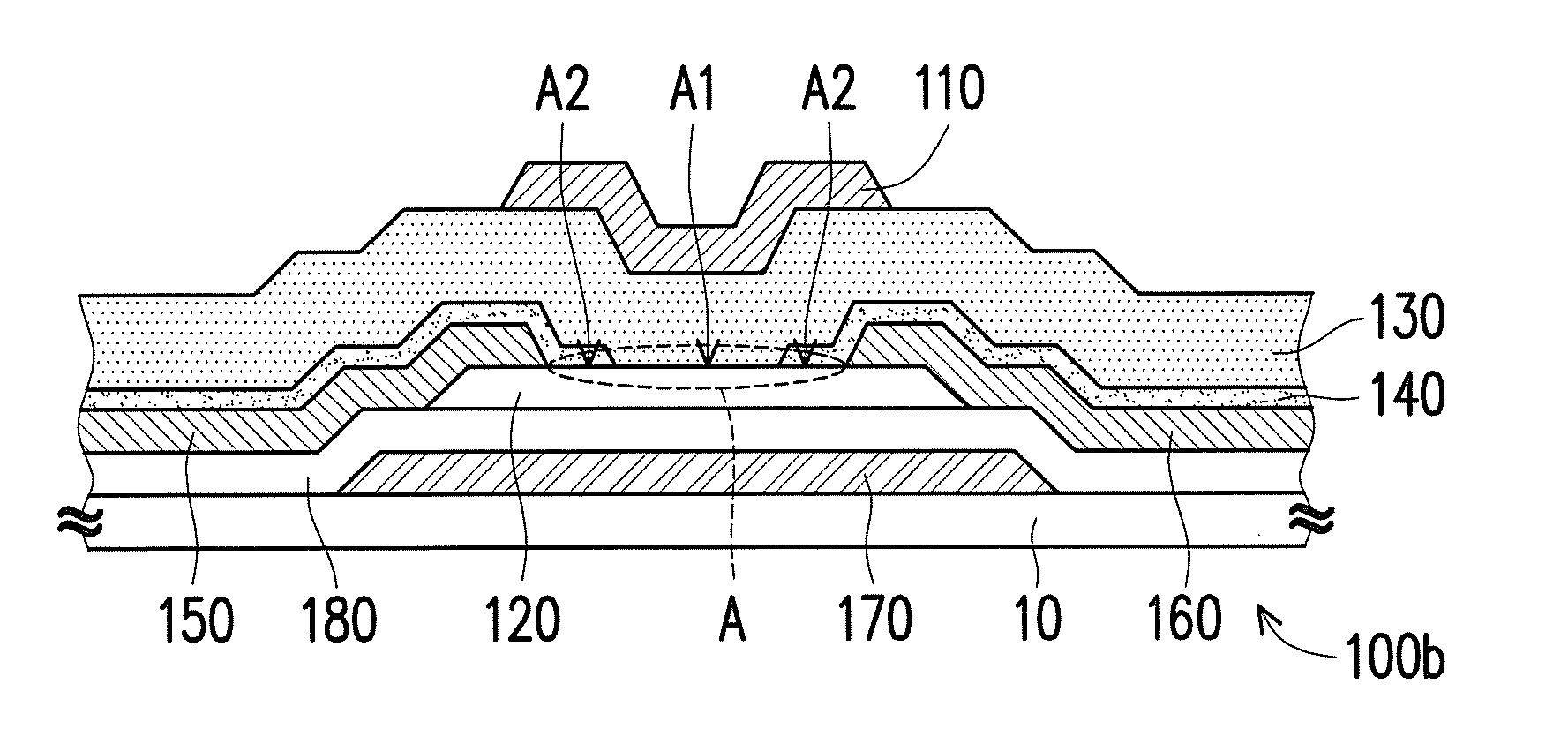
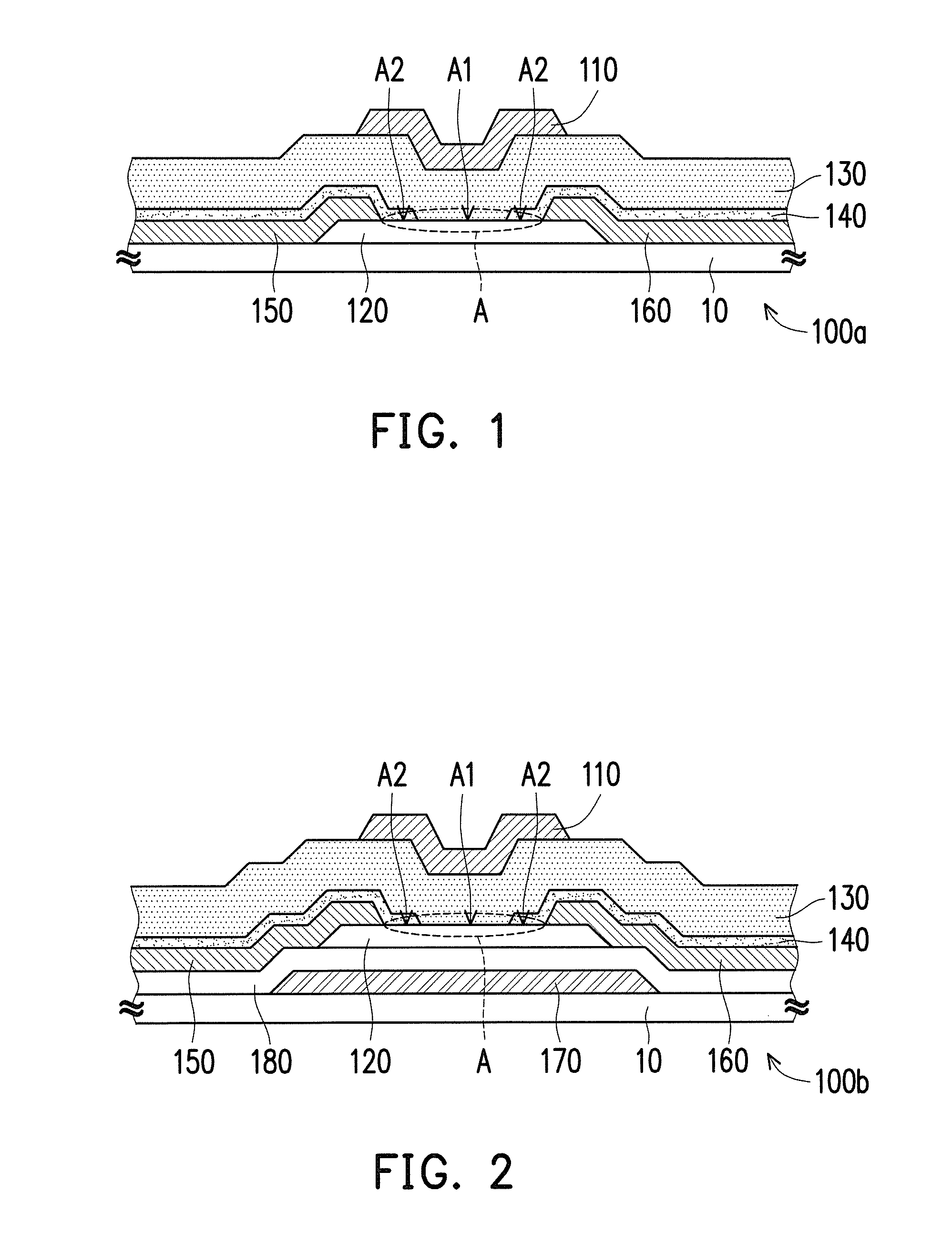
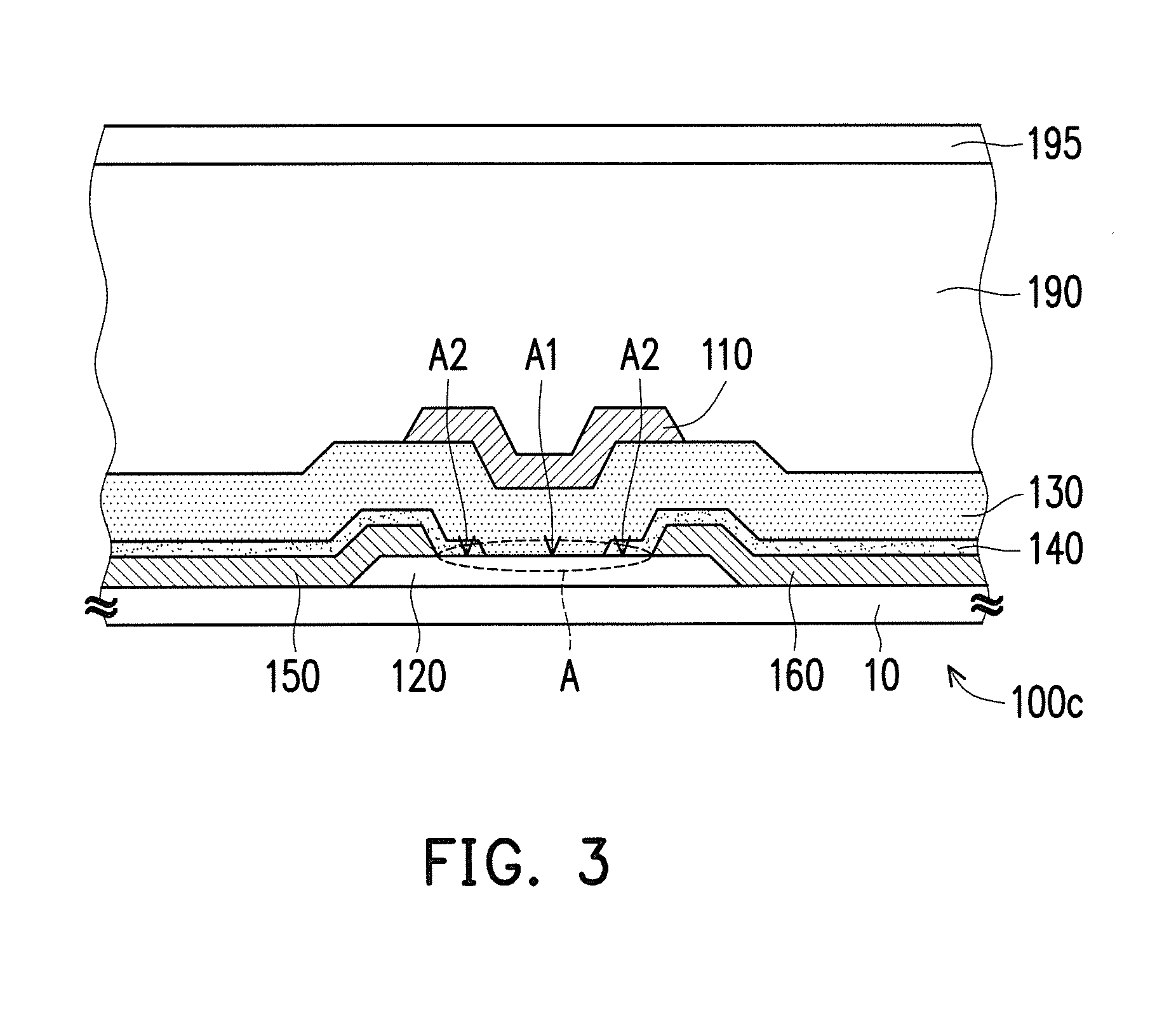
[0023]FIG. 1 is a schematic cross-sectional view of a semiconductor structure according to an embodiment of the application. Referring to FIG. 1, in the current exemplary embodiment, a semiconductor structure 100a is disposed on a substrate 10. The semiconductor structure 100a includes a top gate 110, an oxide semiconductor channel layer 120, a first dielectric layer 130, a second dielectric layer 140, and a source 150 and a drain 160. The oxide semiconductor channel layer 120 is disposed between the top gate 110 and the substrate 10. The first dielectric layer 130 is disposed between the top gate 110 and the oxide semiconductor channel layer 120, while the second dielectric layer 140 is disposed between the first dielectric layer 130 and the oxide semiconductor channel layer 120, wherein a dielectric constant of the first dielectric layer 130 is different from a dielectric constant of the second dielectric layer 140. The source 150 and the drain 160 are disposed at two correspondin...


PUM


Abstract

A semiconductor structure includes a top gate, an oxide semiconductor channel layer, a first dielectric layer, a second dielectric layer, a source and a drain. The oxide semiconductor channel layer is disposed between the top gate and a substrate. The first dielectric layer is disposed between the top gate and the oxide semiconductor channel layer. The second dielectric layer is disposed between the first dielectric layer and the oxide semiconductor channel layer. The source and the drain are disposed on two opposite sides of the oxide semiconductor channel layer and located between the first dielectric layer and the substrate. A portion of the oxide semiconductor channel layer is exposed between the source and the drain. A portion of the first dielectric layer and a portion of the second dielectric layer directly contact with and entirely cover the portion of the oxide semiconductor channel layer.

Description

CROSS-REFERENCE TO RELATED APPLICATION[0001]This application claims the priority benefit of Taiwan application serial no. 103101770, filed on Jan. 17, 2014. The entirety of the above-mentioned patent application is hereby incorporated by reference herein and made a part of this specification.BACKGROUND OF THE INVENTION[0002]1. Field of the Invention[0003]The application relates to a semiconductor structure, and more particularly to a semiconductor structure having an oxide semiconductor channel layer.[0004]2. Description of Related Art[0005]Currently, the most ubiquitous type of liquid crystal display is mainly constructed with a thin film transistor array substrate, a color filter substrate and a liquid crystal layer sandwiched therebetween. On a conventional thin film transistor array substrate, amorphous silicon (a-Si) thin film transistor or low temperature polysilicon thin film transistor is typically used as a switching unit of each sub-pixel. In recent years, many studies hav...

Claims


Application Information

Patent Timeline
IPC IPC(8): H01L29/51H01L29/49H01L29/786
CPCH01L29/513H01L29/7869H01L29/78648H01L29/78609H01L29/4908H01L29/06H01L29/0607H01L29/786
Inventor CHEN, WEI-TSUNGTSAI, CHUANG-CHUANGSHINN, TED-HONGTSAI, XUE-HUNGYANG, CHIH-HSIANG
Owner E INK HLDG INC
Why Eureka
Try Eureka