Integrated circuits with metal-insulator-semiconductor (MIS) contact structures and methods for fabricating same

a technology of metal-insulator and semiconductor, applied in the direction of semiconductor devices, electrical devices, transistors, etc., can solve the problems of limiting factors in the continued shrinkage of integrated semiconductor devices, the resistance of contacts to doped regions, and the decrease of the drive current of devices, so as to improve the performance of devices

Active Publication Date: 2015-07-30
GLOBALFOUNDRIES US INC
View PDF5 Cites 42 Cited by
  • Summary
  • Abstract
  • Description
  • Claims
  • Application Information

AI Technical Summary

Problems solved by technology

However, one of the limiting factors in the continued shrinking of integrated semiconductor devices is the resistance of contacts to doped regions such as the source and drain regions.
In turn, as the resistance of the contacts increases, the drive current of the devices decreases, thus adversely affecting device performance.
MIS contact structure may reduce the barrier height between the semiconductor and the metal contact structures, leading to lower contact resistance despite the additional resistance presented by the thin dielectric insulator layer.

Method used


Image

  • Integrated circuits with metal-insulator-semiconductor (MIS) contact structures and methods for fabricating same
  • Integrated circuits with metal-insulator-semiconductor (MIS) contact structures and methods for fabricating same
  • Integrated circuits with metal-insulator-semiconductor (MIS) contact structures and methods for fabricating same

Examples


Embodiment Construction

[0012]The following detailed description is merely exemplary in nature and is not intended to limit the integrated circuits or the methods for fabricating integrated circuits as claimed herein. Furthermore, there is no intention to be bound by any expressed or implied theory presented in the preceding technical field, background or brief summary, or in the following detailed description.

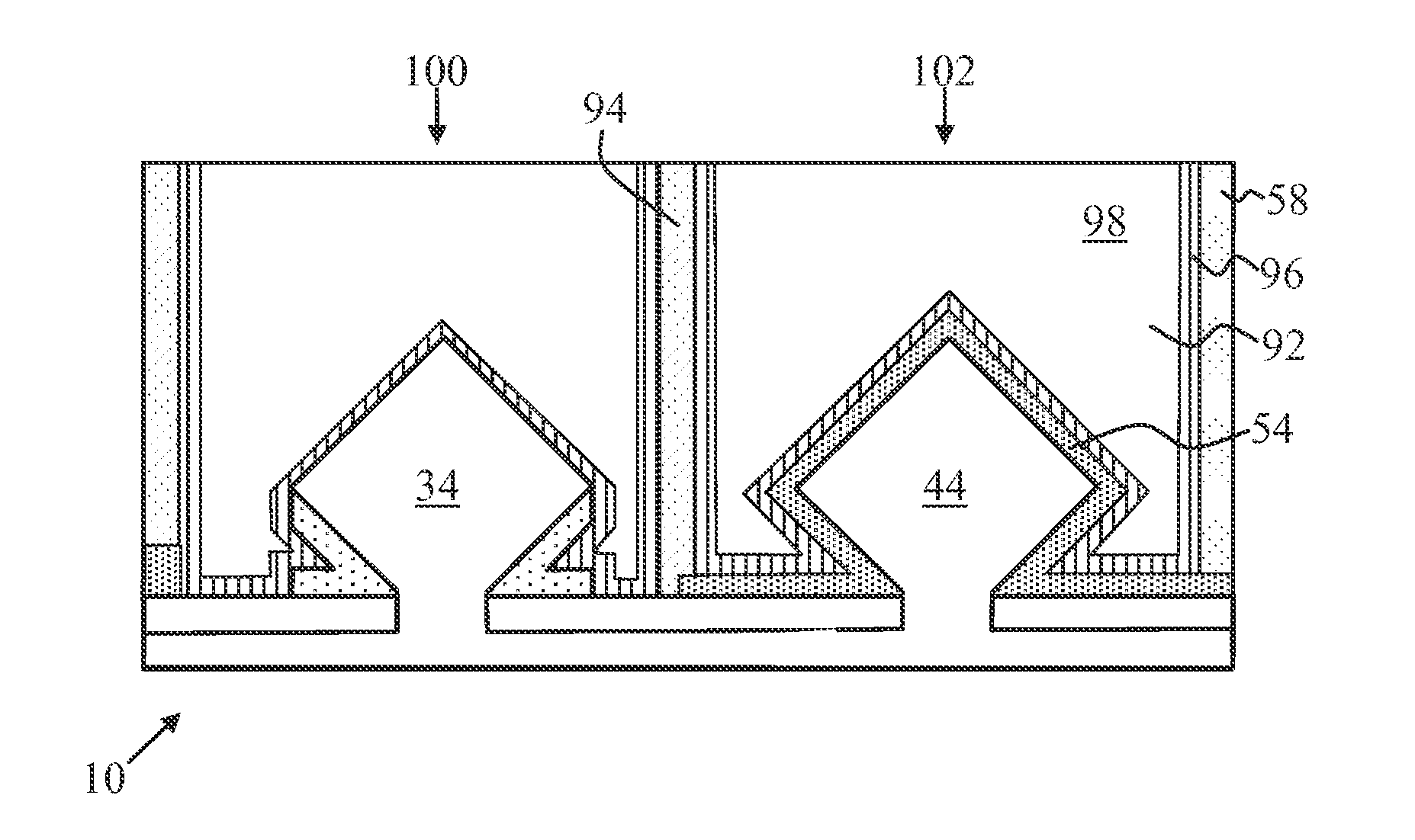
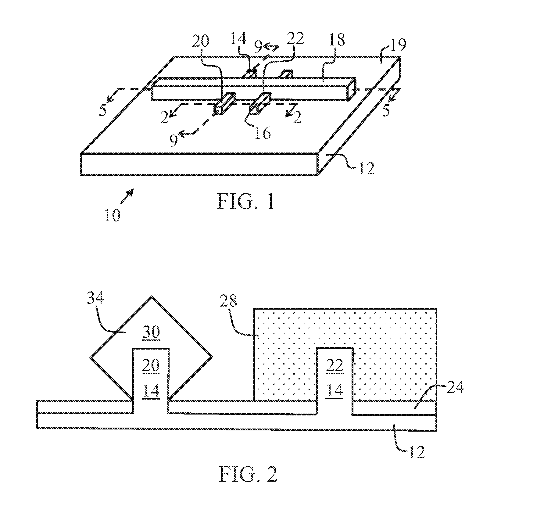
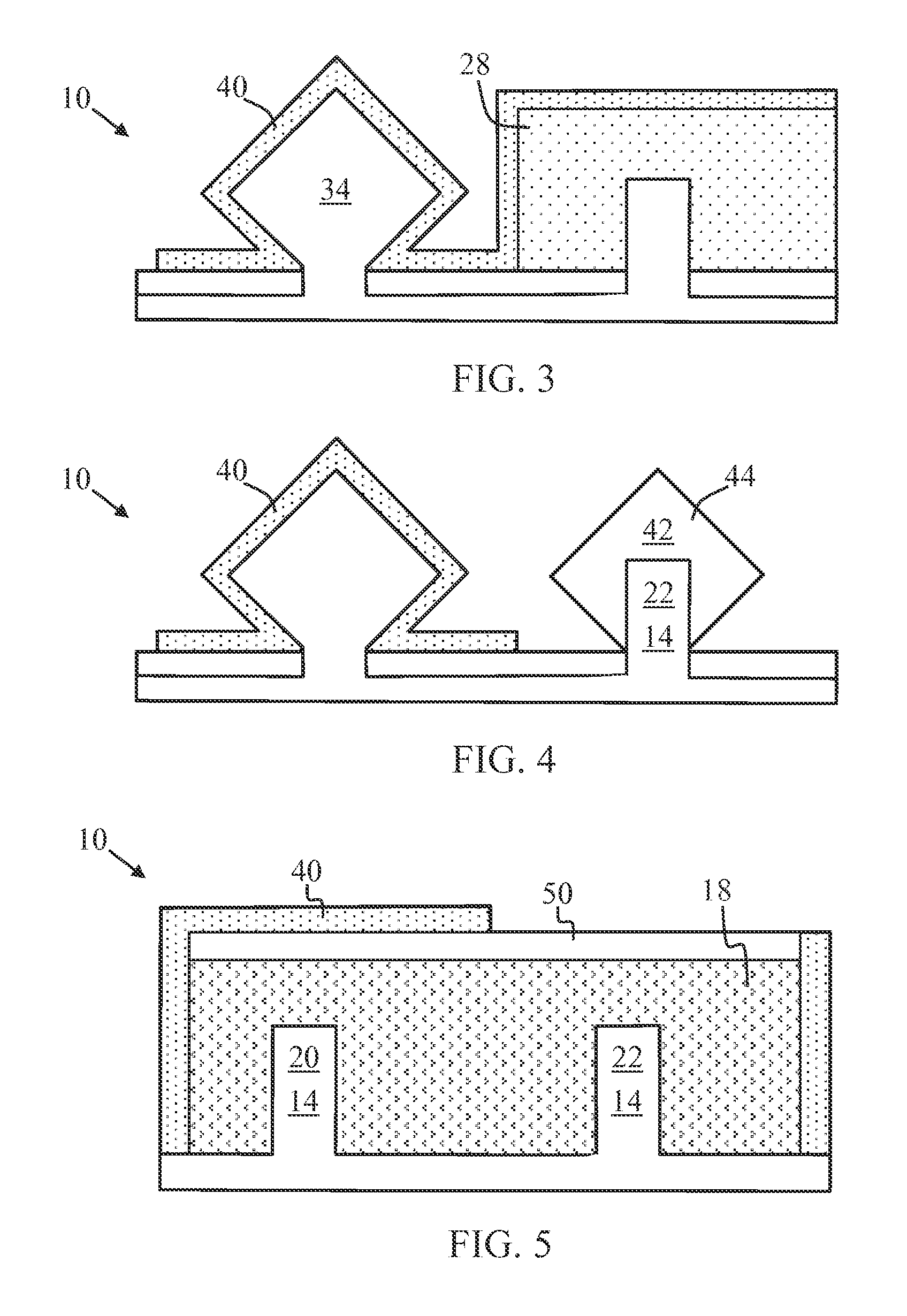
[0013]In accordance with the various embodiments herein, integrated circuits having metal-insulator-semiconductor (MIS) contact structures and methods for fabricating integrated circuits having metal-insulator-semiconductor (MIS) contact structures are provided. Specifically, integrated circuits described herein are provided with metal-insulator-semiconductor contact structures in PFET source / drain regions and metal-semiconductor contact structures in NFET source / drain regions. In exemplary embodiments, the PFET source / drain regions and NFET source / drain regions are formed in and / or on semiconductor ...


PUM


Abstract

Integrated circuits having metal-insulator-semiconductor (MIS) contact structures and methods for fabricating integrated circuits having metal-insulator-semiconductor (MIS) contact structures are provided. In an embodiment, a method for fabricating an integrated circuit includes providing a fin structure formed from semiconductor material overlying a semiconductor substrate. The method includes depositing a layer of high-k dielectric material over the fin structure. Further, the method includes forming a metal layer or layers over the layer of high-k dielectric material to provide the fin structure with a metal-insulator-semiconductor (MIS) contact structure.

Description

TECHNICAL FIELD[0001]The present disclosure generally relates to integrated circuits and methods for fabricating integrated circuits, and more particularly relates to integrated circuits having metal-insulator-semiconductor contact structures and methods for fabricating integrated circuits having metal-insulator-semiconductor contact structures.BACKGROUND[0002]The majority of present day integrated circuits are implemented by using a plurality of interconnected field effect transistors (FETs). Typical transistor devices include gate electrodes as control electrodes that are formed overlying a semiconductor substrate, and spaced-apart source and drain regions that are formed within the semiconductor substrate and between which currents can flow. For a transistor device, a control voltage may be applied to the gate electrode and control the flow of current through a channel in the semiconductor substrate between the source and drain regions and beneath the gate electrode.[0003]A trans...

Claims


Application Information

Patent Timeline
Patent Type & Authority Applications(United States)
IPC IPC(8): H01L21/28H01L27/092H01L21/8238
CPCH01L21/2807H01L27/0924H01L21/823821H01L21/28158H01L21/845H01L29/41791H01L29/66545H01L29/66795H01L27/1211
Inventor BOUCHE, GUILLAUMEKOH, SHAO MINGWAHL, JEREMY A.WEI, ANDY C.
Owner GLOBALFOUNDRIES US INC
Why Eureka
Try Eureka