Method of producing image pick-up apparatus and image pick-up apparatus

US20150214269A1Active Publication Date: 2015-07-30CANON KK

Image

  • Method of producing image pick-up apparatus and image pick-up apparatus
  • Method of producing image pick-up apparatus and image pick-up apparatus
  • Method of producing image pick-up apparatus and image pick-up apparatus

Examples


Embodiment Construction

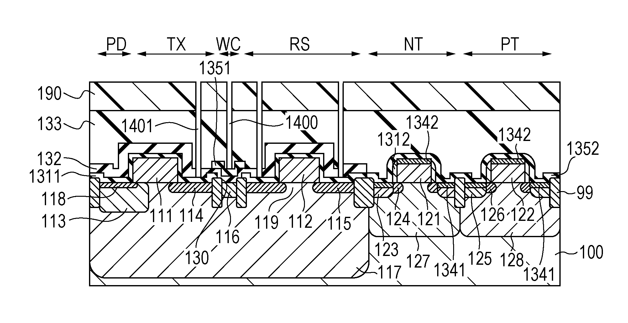
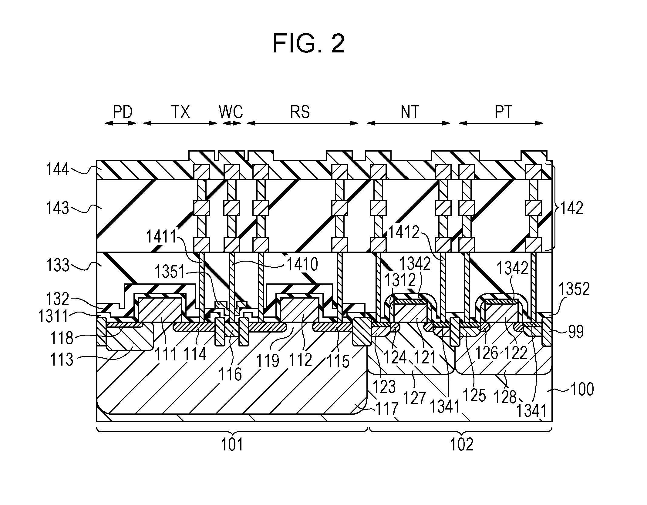
[0017]Embodiments of the present invention will now be described in detail by examples with reference to the drawings. The present invention is not limited to the following examples, and combinations and modifications within the gist of the invention are possible. In the following description and the drawings, the compositions that are common to multiple drawings are denoted with the same reference numerals. Accordingly, the common compositions will be described with reference to multiple drawings, and the descriptions of compositions denoted with the same reference numerals are appropriately omitted.

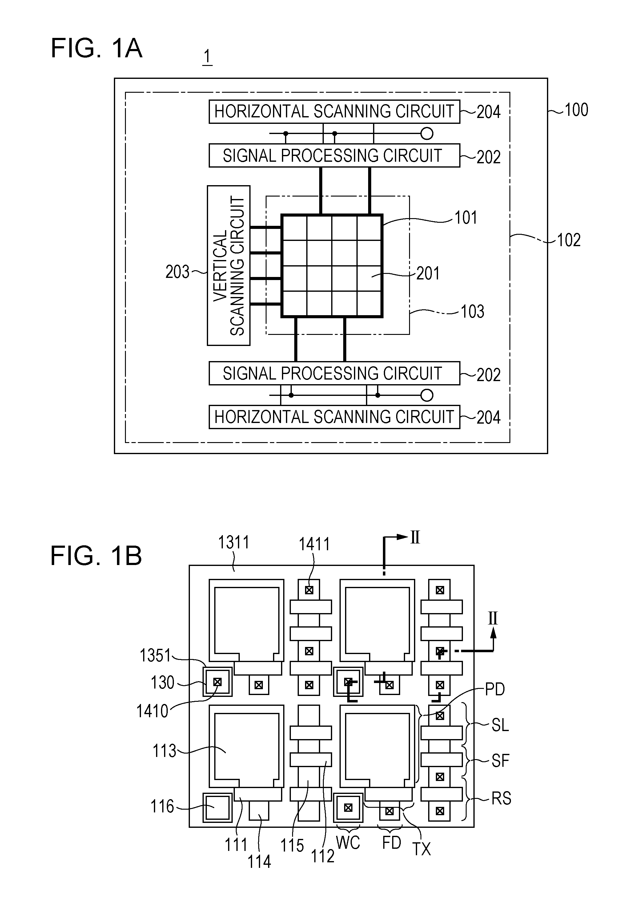
[0018]FIG. 1A shows an example of a schematic planar view of an image pick-up apparatus. The image pick-up apparatus 1 comprises a plurality of pixels each forming a part of an image. The pixel includes one or more photoelectric conversion elements. The pixel may further include a pixel optical system. In such a case, the photoelectric conversion element of the pixel corresponds to a si...


PUM


Abstract

The method comprises forming a first silicon nitride film covering a pixel circuit section by thermal CVD; forming an opening in the first silicon nitride film by removing a first portion of the first silicon nitride film while remaining a second portion of the first silicon nitride film; forming a second silicon nitride film covering the opening by plasma CVD; forming an insulating film covering the first silicon nitride film and the second silicon nitride film and covering a peripheral transistor in the peripheral circuit section; and forming a contact plug passing through the insulating film and being in contact with the peripheral transistor.

Description

BACKGROUND OF THE INVENTION[0001]1. Field of the Invention[0002]The present invention relates to an image pick-up apparatus.[0003]2. Description of the Related Art[0004]In an image pick-up apparatus, a silicon nitride film is disposed on a photoelectric conversion element and protects the photoelectric conversion element and prevents reflection.[0005]Japanese Patent Laid-Open No. 2008-041726 describes formation of a silicon nitride film (36a, 36b) in a photoelectric conversion region (101) by plasma chemical vapor deposition (CVD).[0006]Japanese Patent Laid-Open No. 2013-84693 describes formation of a silicon nitride film covering at least a part of a photoelectric conversion portion by low pressure CVD, and also describes the use of hexechlorodisilane as a source gas of the silicon nitride film in the low pressure CVD.[0007]In the formation of a silicon nitride film near a photoelectric conversion element by plasma CVD as in Japanese Patent Laid-Open No. 2008-041726, there is a ris...

Claims


Application Information

Patent Timeline
30 Jul 2015
Publication
US20150214269A1
IPC
H01L27/146
CPC
H01L27/14685; H01L27/14636; H01L27/14616; H01L21/0217; H01L21/02321; H01L21/76829; H01L21/76832; H01L27/14612
Inventors
ENDO, NOBUYUKI